- 您现在的位置:买卖IC网 > PDF目录10243 > AD7853LARS-REEL (Analog Devices Inc)IC ADC 12BIT SRL 200KSPS 24-SSOP PDF资料下载
参数资料
| 型号: | AD7853LARS-REEL |
| 厂商: | Analog Devices Inc |
| 文件页数: | 17/34页 |
| 文件大小: | 0K |
| 描述: | IC ADC 12BIT SRL 200KSPS 24-SSOP |
| 标准包装: | 1,500 |
| 位数: | 12 |
| 采样率(每秒): | 100k |
| 数据接口: | 8051,QSPI?,串行,SPI? µP |
| 转换器数目: | 2 |
| 功率耗散(最大): | 33mW |
| 电压电源: | 模拟和数字 |
| 工作温度: | -40°C ~ 85°C |
| 安装类型: | 表面贴装 |
| 封装/外壳: | 24-SSOP(0.209",5.30mm 宽) |
| 供应商设备封装: | 24-SSOP |
| 包装: | 带卷 (TR) |
| 输入数目和类型: | 1 个伪差分,单极;1 个伪差分,双极 |
第1页第2页第3页第4页第5页第6页第7页第8页第9页第10页第11页第12页第13页第14页第15页第16页当前第17页第18页第19页第20页第21页第22页第23页第24页第25页第26页第27页第28页第29页第30页第31页第32页第33页第34页
REV. B
–24–
AD7853/AD7853L
DETAILED TIMING SECTION
Mode 1 (2-Wire 8051 Interface)
The read and writing takes place on the DIN line and the con-
version is initiated by pulsing the
CONVST pin (note that in
every write cycle the 2/
3 Mode bit must be set to 1). The con-
version may be started by setting the
CONVST bit in the con-
trol register to 1 instead of using the
CONVST line.
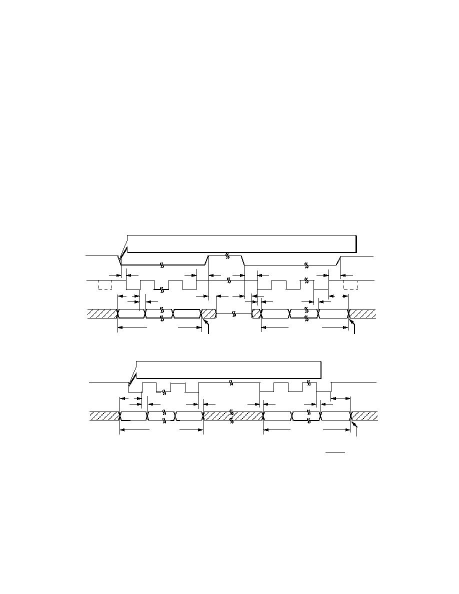
Below in Figure 33 and in Figure 34 are the timing diagrams for
Interface Mode 1 in Table X where we are in the 2-wire inter-
face mode. Here the DIN pin is used for both input and output
as shown. The
SYNC input is level triggered active low and can
be pulsed (Figure 33) or can be constantly low (Figure 34).
In Figure 33 the part samples the input data on the rising edge
of SCLK. After the 16th rising edge of SCLK the DIN is con-
figured as an output. When the
SYNC is taken high the DIN is
three-stated. Taking
SYNC low disables the three-state on the
DIN pin and the first SCLK falling edge clocks out the first data
bit. Once the 16 clocks have been provided the DIN pin will
automatically revert back to an input after a time t14. Note that a
continuous SCLK shown by the dotted waveform in Figure 33
can be used provided that the
SYNC is low for only 16 clock
pulses in each of the read and write cycles. The POLARITY pin
may be used to change the SCLK edge which the data is sampled
on and clocked out on.
In Figure 34 the
SYNC line is tied low permanently and this
results in a different timing arrangement. With
SYNC tied low
permanently the DIN pin will never be three-stated. The 16th
rising edge of SCLK configures the DIN pin as an input or an
output as shown in the diagram. Here no more than 16 SCLK
pulses must occur for each of the read and write operations.
If reading from and writing to the calibration registers in this
interface mode, all the selected calibration registers must be
read from or written to. The read and write operations cannot
be aborted. When reading from the calibration registers, the
DIN pin will remain as an output for the full duration of all the
calibration register read operations. When writing to the calibra-
tion registers, the DIN pin will remain as an input for the full
duration of all the calibration register write operations.
SCLK (I/P)
SYNC (I/P)
t
3
t
8
DIN (I/O)
DB15
DB0
t
3
t
11
t
6
POLARITY PIN
LOGIC HIGH
116
16
1
t
5A
t
12
DIN BECOMES AN INPUT
DB15
THREE-STATE
DATA READ
DATA WRITE
t
7
t
6
t
14
t
11
DIN BECOMES AN OUTPUT
t
3 = –0.4 tSCLK MIN (NONCONTINUOUS SCLK) –/+0.4 tSCLK MIN/MAX (CONTINUOUS SCLK),
t
6 = 75/115 MAX (5V/3V), t7 = 40/60ns MIN (5V/3V), t8 = 20/30 MIN (5V/3V)
Figure 33. Timing Diagram for Read/Write Operation with DIN as an Input/Output (i.e., Interface Mode 1, SM1 = SM2 = 0)
SCLK (I/P)
t
8
DIN (I/O)
DB15
DB0
t
6
116
16
1
DIN BECOMES AN INPUT
DB15
DATA READ
DATA WRITE
t
7
t
6
t
14
t
6 = 75/115 MAX (5V/3V), t7 = 40/60ns MIN (5V/3V), t8 = 20/30 MIN (5V/3V),
t
13 = 90/130 MAX (5V/3V), t14 = 50/90ns MAX (5V/3V)
6
t
13
POLARITY PIN
LOGIC HIGH
Figure 34. Timing Diagram for Read/Write Operation with DIN as an Input/Output and SYNC Input Tied Low
(i.e., Interface Mode 1, SM1 = SM2 = 0)
相关PDF资料 |
PDF描述 |
|---|---|
| VE-23T-CU-F4 | CONVERTER MOD DC/DC 6.5V 200W |
| VE-B2M-MW-F4 | CONVERTER MOD DC/DC 10V 100W |
| VI-26F-MY | CONVERTER MOD DC/DC 72V 50W |
| VE-B2M-MW-F3 | CONVERTER MOD DC/DC 10V 100W |
| VE-23R-IW-S | CONVERTER MOD DC/DC 7.5V 100W |
相关代理商/技术参数 |
参数描述 |
|---|---|
| AD7853LARSZ | 功能描述:IC ADC 12BIT SRL 200KSPS 24SSOP RoHS:是 类别:集成电路 (IC) >> 数据采集 - 模数转换器 系列:- 标准包装:1,000 系列:- 位数:12 采样率(每秒):300k 数据接口:并联 转换器数目:1 功率耗散(最大):75mW 电压电源:单电源 工作温度:0°C ~ 70°C 安装类型:表面贴装 封装/外壳:24-SOIC(0.295",7.50mm 宽) 供应商设备封装:24-SOIC 包装:带卷 (TR) 输入数目和类型:1 个单端,单极;1 个单端,双极 |
| AD7853LARSZ-REEL | 功能描述:IC ADC 12BIT SRL 200KSPS 24SSOP RoHS:是 类别:集成电路 (IC) >> 数据采集 - 模数转换器 系列:- 标准包装:1,000 系列:- 位数:16 采样率(每秒):45k 数据接口:串行 转换器数目:2 功率耗散(最大):315mW 电压电源:模拟和数字 工作温度:0°C ~ 70°C 安装类型:表面贴装 封装/外壳:28-SOIC(0.295",7.50mm 宽) 供应商设备封装:28-SOIC W 包装:带卷 (TR) 输入数目和类型:2 个单端,单极 |
| AD7853LARZ | 功能描述:IC ADC 12BIT SRL 200KSPS 24SOIC RoHS:是 类别:集成电路 (IC) >> 数据采集 - 模数转换器 系列:- 标准包装:1,000 系列:- 位数:12 采样率(每秒):300k 数据接口:并联 转换器数目:1 功率耗散(最大):75mW 电压电源:单电源 工作温度:0°C ~ 70°C 安装类型:表面贴装 封装/外壳:24-SOIC(0.295",7.50mm 宽) 供应商设备封装:24-SOIC 包装:带卷 (TR) 输入数目和类型:1 个单端,单极;1 个单端,双极 |
| AD7853LARZ-REEL | 功能描述:IC ADC 12BIT SRL 200KSPS 24SOIC RoHS:是 类别:集成电路 (IC) >> 数据采集 - 模数转换器 系列:- 产品培训模块:Lead (SnPb) Finish for COTS Obsolescence Mitigation Program 标准包装:2,500 系列:- 位数:12 采样率(每秒):3M 数据接口:- 转换器数目:- 功率耗散(最大):- 电压电源:- 工作温度:- 安装类型:表面贴装 封装/外壳:SOT-23-6 供应商设备封装:SOT-23-6 包装:带卷 (TR) 输入数目和类型:- |
| AD7853LBN | 功能描述:IC ADC 12BIT SRL 200KSPS 24-DIP RoHS:否 类别:集成电路 (IC) >> 数据采集 - 模数转换器 系列:- 标准包装:1,000 系列:- 位数:12 采样率(每秒):300k 数据接口:并联 转换器数目:1 功率耗散(最大):75mW 电压电源:单电源 工作温度:0°C ~ 70°C 安装类型:表面贴装 封装/外壳:24-SOIC(0.295",7.50mm 宽) 供应商设备封装:24-SOIC 包装:带卷 (TR) 输入数目和类型:1 个单端,单极;1 个单端,双极 |
发布紧急采购,3分钟左右您将得到回复。