- 您现在的位置:买卖IC网 > PDF目录10243 > AD7853LARS-REEL (Analog Devices Inc)IC ADC 12BIT SRL 200KSPS 24-SSOP PDF资料下载
参数资料
| 型号: | AD7853LARS-REEL |
| 厂商: | Analog Devices Inc |
| 文件页数: | 7/34页 |
| 文件大小: | 0K |
| 描述: | IC ADC 12BIT SRL 200KSPS 24-SSOP |
| 标准包装: | 1,500 |
| 位数: | 12 |
| 采样率(每秒): | 100k |
| 数据接口: | 8051,QSPI?,串行,SPI? µP |
| 转换器数目: | 2 |
| 功率耗散(最大): | 33mW |
| 电压电源: | 模拟和数字 |
| 工作温度: | -40°C ~ 85°C |
| 安装类型: | 表面贴装 |
| 封装/外壳: | 24-SSOP(0.209",5.30mm 宽) |
| 供应商设备封装: | 24-SSOP |
| 包装: | 带卷 (TR) |
| 输入数目和类型: | 1 个伪差分,单极;1 个伪差分,双极 |
第1页第2页第3页第4页第5页第6页当前第7页第8页第9页第10页第11页第12页第13页第14页第15页第16页第17页第18页第19页第20页第21页第22页第23页第24页第25页第26页第27页第28页第29页第30页第31页第32页第33页第34页
REV. B
–15–
AD7853/AD7853L
DC/AC Applications
For dc applications high source impedances are acceptable,
provided there is enough acquisition time between conversions
to charge the 20 pF capacitor. The acquisition time can be
calculated from the above formula for different source imped-
ances. For example with RIN = 5 k
, the required acquisition
time will be 922 ns.
For ac applications, removing high frequency components from
the analog input signal is recommended by use of an RC low-
pass filter on the AIN(+) pin, as shown in Figure 13. In applica-
tions where harmonic distortion and signal to noise ratio are
critical, the analog input should be driven from a low impedance
source. Large source impedances will significantly affect the ac
performance of the ADC. This may necessitate the use of an
input buffer amplifier. The choice of the op amp will be a func-
tion of the particular application.
When no amplifier is used to drive the analog input the source
impedance should be limited to low values. The maximum
source impedance will depend on the amount of total harmonic
distortion (THD) that can be tolerated. The THD will increase
as the source impedance increases and performance will degrade.
Figure 12 shows a graph of the Total Harmonic Distortion vs.
analog input signal frequency for different source impedances.
With the setup as in Figure 13, the THD is at the –90 dB level.
With a source impedance of 1 k
and no capacitor on the AIN(+)
pin, the THD increases with frequency.
INPUT FREQUENCY – kHz
–72
–76
–92
0
100
THD
–
dB
20
40
60
80
–80
–84
–88
RIN = 1k
RIN = 50 , 10nF
AS IN FIGURE 13
THD VS. FREQUENCY FOR DIFFERENT
SOURCE IMPEDANCES
Figure 12. THD vs. Analog Input Frequency
In a single supply application (both 3 V and 5 V), the V+ and
V– of the op amp can be taken directly from the supplies to the
AD7853/AD7853L which eliminates the need for extra external
power supplies. When operating with rail-to-rail inputs and
outputs at frequencies greater than 10 kHz, care must be taken
in selecting the particular op amp for the application. In particu-
lar, for single supply applications the input amplifiers should be
connected in a gain of –1 arrangement to get the optimum per-
formance. Figure 13 shows the arrangement for a single supply
application with a 50
and 10 nF low-pass filter (cutoff fre-
quency 320 kHz) on the AIN(+) pin. Note that the 10 nF is a
capacitor with good linearity to ensure good ac performance.
Recommended single supply op amps are the AD820 and the
AD820-3 V.
TYPICAL CONNECTION DIAGRAM
Figure 10 shows a typical connection diagram for the AD7853/
AD7853L. The DIN line is tied to DGND so that no data is
written to the part. The AGND and the DGND pins are con-
nected together at the device for good noise suppression. The
CAL pin has a 0.01
F capacitor to enable an automatic self-
calibration on power-up. The SCLK and
SYNC are configured
as outputs by having SM1 and SM2 at DVDD. The conversion
result is output in a 16-bit word with four leading zeros followed
by the MSB of the 12-bit result. Note that after the AVDD and
DVDD power-up, the part will require approximately 150 ms for
the internal reference to settle and for the automatic calibration
on power-up to be completed.
For applications where power consumption is a major concern,
the
SLEEP pin can be connected to DGND. See Power-Down
section for more detail on low power applications.
ANALOG INPUT
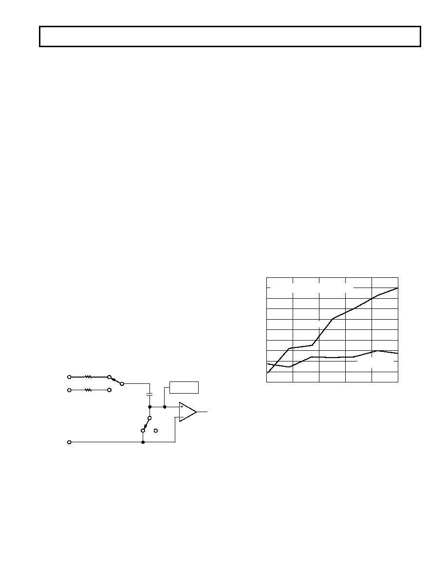
The equivalent circuit of the analog input section is shown in
Figure 11. During the acquisition interval the switches are both
in the track position and the AIN(+) charges the 20 pF capaci-
tor through the 125
resistance. On the rising edge of CONVST
switches SW1 and SW2 go into the hold position retaining
charge on the 20 pF capacitor as a sample of the signal on
AIN(+). The AIN(–) is connected to the 20 pF capacitor, and
this unbalances the voltage at Node A at the input of the com-
parator. The capacitor DAC adjusts during the remainder of the
conversion cycle to restore the voltage at Node A to the correct
value. This action transfers a charge, representing the analog
input signal, to the capacitor DAC which in turn forms a digital
representation of the analog input signal. The voltage on the
AIN(–) pin directly influences the charge transferred to the
capacitor DAC at the hold instant. If this voltage changes dur-
ing the conversion period, the DAC representation of the analog
input voltage will be altered. Therefore it is most important that
the voltage on the AIN(–) pin remains constant during the con-
version period. Furthermore, it is recommended that the AIN(–)
pin is always connected to AGND or to a fixed dc voltage.
AIN(+)
AIN(–)
125
20pF
TRACK
HOLD
CAPACITOR
DAC
COMPARATOR
HOLD
TRACK
CREF2
125
SW1
SW2
NODE A
Figure 11. Analog Input Equivalent Circuit
Acquisition Time
The track and hold amplifier enters its tracking mode on the
falling edge of the BUSY signal. The time required for the track
and hold amplifier to acquire an input signal will depend on
how quickly the 20 pF input capacitance is charged. The acqui-
sition time is calculated using the formula:
tACQ = 9
× (R
IN + 125
) × 20 pF
where RIN is the source impedance of the input signal, and 125
,
20 pF is the input R, C.
相关PDF资料 |
PDF描述 |
|---|---|
| VE-23T-CU-F4 | CONVERTER MOD DC/DC 6.5V 200W |
| VE-B2M-MW-F4 | CONVERTER MOD DC/DC 10V 100W |
| VI-26F-MY | CONVERTER MOD DC/DC 72V 50W |
| VE-B2M-MW-F3 | CONVERTER MOD DC/DC 10V 100W |
| VE-23R-IW-S | CONVERTER MOD DC/DC 7.5V 100W |
相关代理商/技术参数 |
参数描述 |
|---|---|
| AD7853LARSZ | 功能描述:IC ADC 12BIT SRL 200KSPS 24SSOP RoHS:是 类别:集成电路 (IC) >> 数据采集 - 模数转换器 系列:- 标准包装:1,000 系列:- 位数:12 采样率(每秒):300k 数据接口:并联 转换器数目:1 功率耗散(最大):75mW 电压电源:单电源 工作温度:0°C ~ 70°C 安装类型:表面贴装 封装/外壳:24-SOIC(0.295",7.50mm 宽) 供应商设备封装:24-SOIC 包装:带卷 (TR) 输入数目和类型:1 个单端,单极;1 个单端,双极 |
| AD7853LARSZ-REEL | 功能描述:IC ADC 12BIT SRL 200KSPS 24SSOP RoHS:是 类别:集成电路 (IC) >> 数据采集 - 模数转换器 系列:- 标准包装:1,000 系列:- 位数:16 采样率(每秒):45k 数据接口:串行 转换器数目:2 功率耗散(最大):315mW 电压电源:模拟和数字 工作温度:0°C ~ 70°C 安装类型:表面贴装 封装/外壳:28-SOIC(0.295",7.50mm 宽) 供应商设备封装:28-SOIC W 包装:带卷 (TR) 输入数目和类型:2 个单端,单极 |
| AD7853LARZ | 功能描述:IC ADC 12BIT SRL 200KSPS 24SOIC RoHS:是 类别:集成电路 (IC) >> 数据采集 - 模数转换器 系列:- 标准包装:1,000 系列:- 位数:12 采样率(每秒):300k 数据接口:并联 转换器数目:1 功率耗散(最大):75mW 电压电源:单电源 工作温度:0°C ~ 70°C 安装类型:表面贴装 封装/外壳:24-SOIC(0.295",7.50mm 宽) 供应商设备封装:24-SOIC 包装:带卷 (TR) 输入数目和类型:1 个单端,单极;1 个单端,双极 |
| AD7853LARZ-REEL | 功能描述:IC ADC 12BIT SRL 200KSPS 24SOIC RoHS:是 类别:集成电路 (IC) >> 数据采集 - 模数转换器 系列:- 产品培训模块:Lead (SnPb) Finish for COTS Obsolescence Mitigation Program 标准包装:2,500 系列:- 位数:12 采样率(每秒):3M 数据接口:- 转换器数目:- 功率耗散(最大):- 电压电源:- 工作温度:- 安装类型:表面贴装 封装/外壳:SOT-23-6 供应商设备封装:SOT-23-6 包装:带卷 (TR) 输入数目和类型:- |
| AD7853LBN | 功能描述:IC ADC 12BIT SRL 200KSPS 24-DIP RoHS:否 类别:集成电路 (IC) >> 数据采集 - 模数转换器 系列:- 标准包装:1,000 系列:- 位数:12 采样率(每秒):300k 数据接口:并联 转换器数目:1 功率耗散(最大):75mW 电压电源:单电源 工作温度:0°C ~ 70°C 安装类型:表面贴装 封装/外壳:24-SOIC(0.295",7.50mm 宽) 供应商设备封装:24-SOIC 包装:带卷 (TR) 输入数目和类型:1 个单端,单极;1 个单端,双极 |
发布紧急采购,3分钟左右您将得到回复。