- 您现在的位置:买卖IC网 > PDF目录10243 > AD7853LARS-REEL (Analog Devices Inc)IC ADC 12BIT SRL 200KSPS 24-SSOP PDF资料下载
参数资料
| 型号: | AD7853LARS-REEL |
| 厂商: | Analog Devices Inc |
| 文件页数: | 8/34页 |
| 文件大小: | 0K |
| 描述: | IC ADC 12BIT SRL 200KSPS 24-SSOP |
| 标准包装: | 1,500 |
| 位数: | 12 |
| 采样率(每秒): | 100k |
| 数据接口: | 8051,QSPI?,串行,SPI? µP |
| 转换器数目: | 2 |
| 功率耗散(最大): | 33mW |
| 电压电源: | 模拟和数字 |
| 工作温度: | -40°C ~ 85°C |
| 安装类型: | 表面贴装 |
| 封装/外壳: | 24-SSOP(0.209",5.30mm 宽) |
| 供应商设备封装: | 24-SSOP |
| 包装: | 带卷 (TR) |
| 输入数目和类型: | 1 个伪差分,单极;1 个伪差分,双极 |
第1页第2页第3页第4页第5页第6页第7页当前第8页第9页第10页第11页第12页第13页第14页第15页第16页第17页第18页第19页第20页第21页第22页第23页第24页第25页第26页第27页第28页第29页第30页第31页第32页第33页第34页
REV. B
–16–
AD7853/AD7853L
AIN(+)
AIN(–)
AMODE
AD7853/AD7853L
BIPOLAR
ANALOG
INPUT RANGE
SELECTED
DOUT
2S
COMPLEMENT
FORMAT
VIN = 0 TO VREF
TRACK AND HOLD
AMPLIFIER
VREF/2
DVDD
Figure 15.
±V
REF/2 about VREF/2 Bipolar Input Configuration
+FS –1LSB
OUTPUT
CODE
0V
111...111
111...110
111...101
111...100
000...011
000...001
000...000
000...010
VIN = (AIN(+) – AIN(–)), INPUT VOLTAGE
1LSB
1LSB =
FS
4096
Figure 16. Unipolar Transfer Characteristic
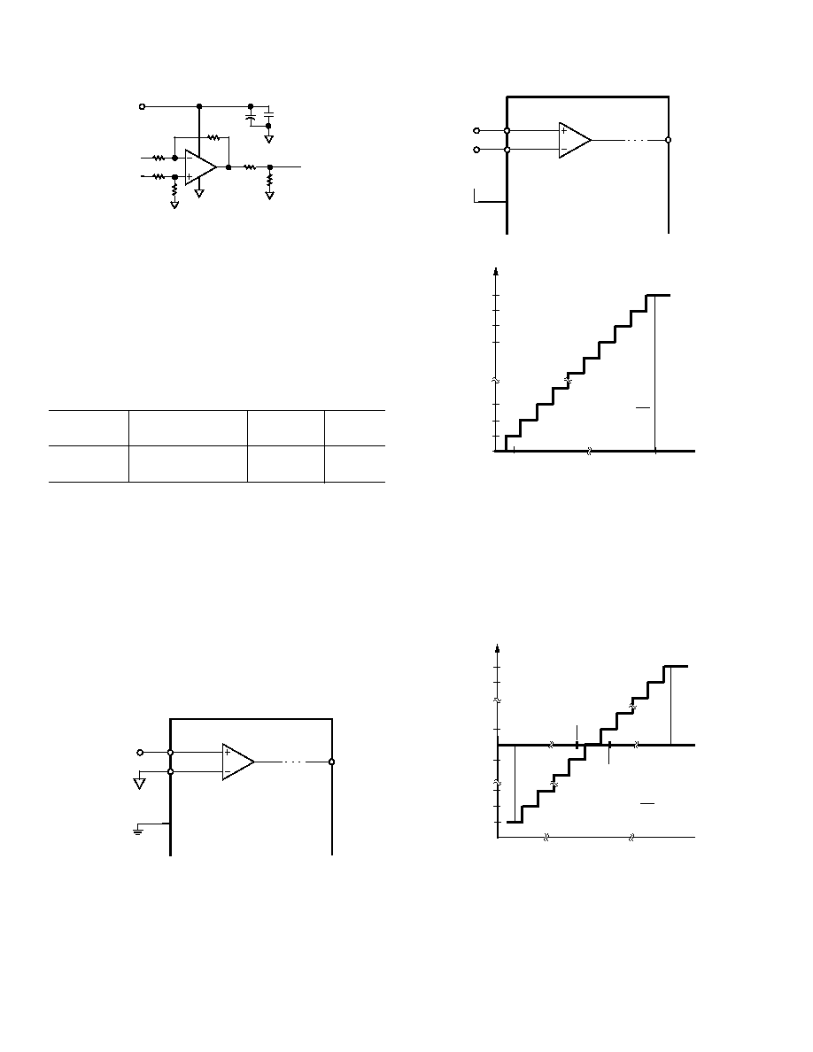
Figure 15 shows the AD7853/AD7853L’s
±V
REF/2 bipolar ana-
log input configuration (where AIN(+) cannot go below 0 V so
for the full bipolar range then the AIN(–) pin should be biased
to +VREF/2). Once again the designed code transitions occur
midway between successive integer LSB values. The output
coding is twos complement with 1 LSB = 4096 = 3.3 V/4096 =
0.8 mV. The ideal input/output transfer characteristic is shown
in Figure 17.
– 1 LSB
FS = VREFV
1LSB =
FS
4096
OUTPUT
CODE
VREF/2
011...111
011...110
000...001
000...000
100...001
100...000
100...010
VIN = (AIN(+) – AIN(–)), INPUT VOLTAGE
0V
+ FS
111...111
(VREF/2) –1 LSB
(VREF/2) +1 LSB
Figure 17. Bipolar Transfer Characteristic
IC1
AD820
AD820-3V
0.1 F
10 F
V+
V–
10k
50
10nF
(NPO)
TO AIN(+) OF
AD7853/AD7853L
VIN
–VREF/2 TO +VREF/2
VREF/2
10k
+3V TO +5V
Figure 13. Analog Input Buffering
Input Ranges
The analog input range for the AD7853/AD7853L is 0 V to
VREF in both the unipolar and bipolar ranges.
The only difference between the unipolar range and the bipolar
range is that in the bipolar range the AIN(–) has to be biased up
to +VREF/2 and the output coding is twos complement (See
Table V and Figures 14 and 15). The unipolar or bipolar mode
is selected by the AMODE pin (0 for the unipolar range and 1
for the bipolar range).
Table V. Analog Input Connections
Analog Input
Input Connections Connection
Range
AIN(+)
AIN(–)
Diagram
AMODE
0 V to VREF
1
VIN
AGND
Figure 14
DGND
±V
REF/2
2
VIN
VREF/2
Figure 15
DVDD
NOTES
1Output code format is straight binary.
2Range is
±V
REF/2 biased about VREF/2. Output code format is twos complement.
Note that the AIN(–) pin on the AD7853/AD7853L can be
biased up above AGND in the unipolar mode also, if required.
The advantage of biasing the lower end of the analog input
range away from AGND is that the user does not have to have
the analog input swing all the way down to AGND. This has the
advantage in true single supply applications that the input am-
plifier does not have to swing all the way down to AGND. The
upper end of the analog input range is shifted up by the same
amount. Care must be taken so that the bias applied does not
shift the upper end of the analog input above the AVDD supply.
In the case where the reference is the supply, AVDD, the AIN(–)
must be tied to AGND in unipolar mode.
AIN(+)
AIN(–)
AMODE
AD7853/AD7853L
UNIPOLAR ANALOG
INPUT RANGE
SELECTED
DOUT
STRAIGHT
BINARY
FORMAT
VIN = 0 TO VREF
TRACK AND HOLD
AMPLIFIER
Figure 14. 0 to VREF Unipolar Input Configuration
Transfer Functions
For the unipolar range the designed code transitions occur
midway between successive integer LSB values (i.e., 1/2 LSB,
3/2 LSBs, 5/2 LSBs . . . FS –3/2 LSBs). The output coding is
straight binary for the unipolar range with 1 LSB = FS/4096 =
3.3 V/4096 = 0.8 mV when VREF = 3.3 V. The ideal input/output
transfer characteristic for the unipolar range is shown in
Figure 16.
相关PDF资料 |
PDF描述 |
|---|---|
| VE-23T-CU-F4 | CONVERTER MOD DC/DC 6.5V 200W |
| VE-B2M-MW-F4 | CONVERTER MOD DC/DC 10V 100W |
| VI-26F-MY | CONVERTER MOD DC/DC 72V 50W |
| VE-B2M-MW-F3 | CONVERTER MOD DC/DC 10V 100W |
| VE-23R-IW-S | CONVERTER MOD DC/DC 7.5V 100W |
相关代理商/技术参数 |
参数描述 |
|---|---|
| AD7853LARSZ | 功能描述:IC ADC 12BIT SRL 200KSPS 24SSOP RoHS:是 类别:集成电路 (IC) >> 数据采集 - 模数转换器 系列:- 标准包装:1,000 系列:- 位数:12 采样率(每秒):300k 数据接口:并联 转换器数目:1 功率耗散(最大):75mW 电压电源:单电源 工作温度:0°C ~ 70°C 安装类型:表面贴装 封装/外壳:24-SOIC(0.295",7.50mm 宽) 供应商设备封装:24-SOIC 包装:带卷 (TR) 输入数目和类型:1 个单端,单极;1 个单端,双极 |
| AD7853LARSZ-REEL | 功能描述:IC ADC 12BIT SRL 200KSPS 24SSOP RoHS:是 类别:集成电路 (IC) >> 数据采集 - 模数转换器 系列:- 标准包装:1,000 系列:- 位数:16 采样率(每秒):45k 数据接口:串行 转换器数目:2 功率耗散(最大):315mW 电压电源:模拟和数字 工作温度:0°C ~ 70°C 安装类型:表面贴装 封装/外壳:28-SOIC(0.295",7.50mm 宽) 供应商设备封装:28-SOIC W 包装:带卷 (TR) 输入数目和类型:2 个单端,单极 |
| AD7853LARZ | 功能描述:IC ADC 12BIT SRL 200KSPS 24SOIC RoHS:是 类别:集成电路 (IC) >> 数据采集 - 模数转换器 系列:- 标准包装:1,000 系列:- 位数:12 采样率(每秒):300k 数据接口:并联 转换器数目:1 功率耗散(最大):75mW 电压电源:单电源 工作温度:0°C ~ 70°C 安装类型:表面贴装 封装/外壳:24-SOIC(0.295",7.50mm 宽) 供应商设备封装:24-SOIC 包装:带卷 (TR) 输入数目和类型:1 个单端,单极;1 个单端,双极 |
| AD7853LARZ-REEL | 功能描述:IC ADC 12BIT SRL 200KSPS 24SOIC RoHS:是 类别:集成电路 (IC) >> 数据采集 - 模数转换器 系列:- 产品培训模块:Lead (SnPb) Finish for COTS Obsolescence Mitigation Program 标准包装:2,500 系列:- 位数:12 采样率(每秒):3M 数据接口:- 转换器数目:- 功率耗散(最大):- 电压电源:- 工作温度:- 安装类型:表面贴装 封装/外壳:SOT-23-6 供应商设备封装:SOT-23-6 包装:带卷 (TR) 输入数目和类型:- |
| AD7853LBN | 功能描述:IC ADC 12BIT SRL 200KSPS 24-DIP RoHS:否 类别:集成电路 (IC) >> 数据采集 - 模数转换器 系列:- 标准包装:1,000 系列:- 位数:12 采样率(每秒):300k 数据接口:并联 转换器数目:1 功率耗散(最大):75mW 电压电源:单电源 工作温度:0°C ~ 70°C 安装类型:表面贴装 封装/外壳:24-SOIC(0.295",7.50mm 宽) 供应商设备封装:24-SOIC 包装:带卷 (TR) 输入数目和类型:1 个单端,单极;1 个单端,双极 |
发布紧急采购,3分钟左右您将得到回复。