- 您现在的位置:买卖IC网 > PDF目录10541 > AD7854LARSZ (Analog Devices Inc)IC ADC 12BIT PARALLEL LP 28SSOP PDF资料下载
参数资料
| 型号: | AD7854LARSZ |
| 厂商: | Analog Devices Inc |
| 文件页数: | 10/28页 |
| 文件大小: | 0K |
| 描述: | IC ADC 12BIT PARALLEL LP 28SSOP |
| 标准包装: | 47 |
| 位数: | 12 |
| 采样率(每秒): | 100k |
| 数据接口: | 并联 |
| 转换器数目: | 2 |
| 功率耗散(最大): | 30mW |
| 电压电源: | 模拟和数字 |
| 工作温度: | -40°C ~ 85°C |
| 安装类型: | 表面贴装 |
| 封装/外壳: | 28-SSOP(0.209",5.30mm 宽) |
| 供应商设备封装: | 28-SSOP |
| 包装: | 管件 |
| 输入数目和类型: | 1 个伪差分,单极;1 个伪差分,双极 |
第1页第2页第3页第4页第5页第6页第7页第8页第9页当前第10页第11页第12页第13页第14页第15页第16页第17页第18页第19页第20页第21页第22页第23页第24页第25页第26页第27页第28页
AD7854/AD7854L
–18–
REV. B
Using The Internal (On-Chip) Reference
As in the case of an external reference the AD7854/AD7854L can
power up from one of two conditions, power-up after the sup-
plies are connected or power-up from a software power-down.
When using the on-chip reference and powering up when AVDD
and DVDD are first connected, it is recommended that the power-
up calibration mode be disabled as explained above. When using
the on-chip reference, the power-up time is effectively the time
it takes to charge up the external capacitor on the REFIN/
REFOUT pin. This time is given by the equation:
tUP = 9
× R × C
where R
≈ 150K and C = external capacitor.
The recommended value of the external capacitor is 100 nF;
this gives a power-up time of approximately 135 ms before a
calibration is initiated and normal operation should commence.
When CREF is fully charged, the power-up time from a software
power-down reduces to 5
s. This is because an internal switch
opens to provide a high impedance discharge path for the refer-
ence capacitor during power-down—see Figure 22. An added
advantage of the low charge leakage from the reference capacitor
during power-down is that even though the reference is being
powered down between conversions, the reference capacitor
holds the reference voltage to within 0.5 LSBs with throughput
rates of 100 samples/second and over with a full power-down
between conversions. A high input impedance op amp like the
AD707 should be used to buffer this reference capacitor if it is
being used externally. Note, if the AD7854/AD7854L is left in
its powered-down state for more than 100 ms, the charge on
CREF will start to leak away and the power-up time will increase.
If this longer power-up time is a problem, the user can use a
partial power-down for the last conversion so the reference
remains powered up.
SWITCH OPENS
DURING POWER-DOWN
TO OTHER CIRCUITRY
REFIN/OUT
EXTERNAL
CAPACITOR
ON-CHIP
REFERENCE
BUF
AD7854/
AD7854L
Figure 22. On-Chip Reference During Power-Down
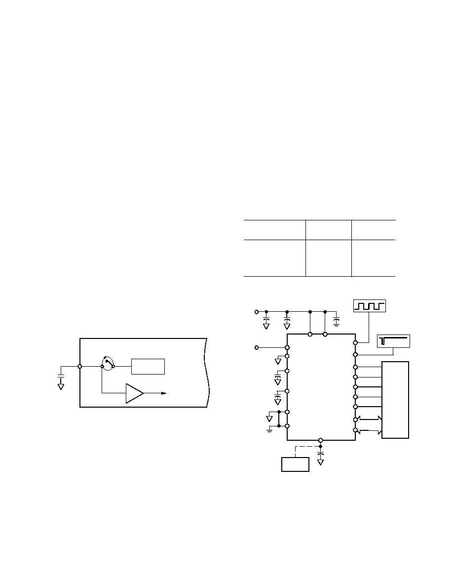
POWER VS. THROUGHPUT RATE
The main advantage of a full power-down after a conversion is
that it significantly reduces the power consumption of the part
at lower throughput rates. When using this mode of operation,
the AD7854/AD7854L is only powered up for the duration of
the conversion. If the power-up time of the AD7854/AD7854L
is taken to be 5
s and it is assumed that the current during
power-up is 4.5 mA/1.5 mA typ, then power consumption as a
function of throughput can easily be calculated. The AD7854
has a conversion time of 4.6
s with a 4 MHz external clock,
and the AD7854L has a conversion time of 9
s with a 1.8 MHz
clock. This means the AD7854/AD7854L consumes 4.5 mA/
1.5 mA typ for 9.6
s/14 s in every conversion cycle if the parts
are powered down at the end of a conversion. The four graphs,
Figures 24, 25, 26 and 27, show the power consumption of the
AD7854 and AD7854L for VDD = 3 V as a function of through-
put. Table VII lists the power consumption for various throughput
rates.
Table VII. Power Consumption vs. Throughput
Power
Throughput Rate
AD7854
AD7854L
1 kSPS
130
W65 W
10 kSPS
1.3 mW
650
W
20 kSPS
2.6 mW
1.25 mW
50 kSPS
6.48 mW
3.2 mW
4MHz/1.8MHz
OSCILLATOR
AVDD DVDD
AIN(+)
AIN(–)
CREF1
CREF2
DB11
DB0
CONVST
AGND
DGND
CLKIN
REFIN/REFOUT
AD7854/
AD7854L
ANALOG
SUPPLY
+3V TO +5V
0.1 F
10 F
0.1 F
0.01 F
CONVERSION
START SIGNAL
0.1nF EXTERNAL REFERENCE
0.1 F ON-CHIP REFERENCE
0V TO 2.5V
INPUT
OPTIONAL
EXTERNAL
REFERENCE
CS
RD
WR
BUSY
AD780/
REF192
C/ P
HBEN
FULL POWER-DOWN
AFTER A CONVERSION
PMGT1 = 0
PMGT0 = 1
Figure 23. Typical Low Power Circuit
相关PDF资料 |
PDF描述 |
|---|---|
| VI-J14-MY-F4 | CONVERTER MOD DC/DC 48V 50W |
| VI-J13-MY-F4 | CONVERTER MOD DC/DC 24V 50W |
| AD7495BRMZ | IC ADC 12BIT SRL LP W/REF 8MSOP |
| AD7495BRZ | IC ADC 12BIT SRL LP W/REF 8-SOIC |
| UTS7124S | CONN RCPT 4X1.6 FEMALE JAM NUT |
相关代理商/技术参数 |
参数描述 |
|---|---|
| AD7854LARSZ-REEL | 功能描述:IC ADC 12BIT PARALLEL LP 28SSOP RoHS:是 类别:集成电路 (IC) >> 数据采集 - 模数转换器 系列:- 标准包装:1,000 系列:- 位数:16 采样率(每秒):45k 数据接口:串行 转换器数目:2 功率耗散(最大):315mW 电压电源:模拟和数字 工作温度:0°C ~ 70°C 安装类型:表面贴装 封装/外壳:28-SOIC(0.295",7.50mm 宽) 供应商设备封装:28-SOIC W 包装:带卷 (TR) 输入数目和类型:2 个单端,单极 |
| AD7854LARZ | 功能描述:IC ADC 12BIT PARALLEL LP 28-SOIC RoHS:是 类别:集成电路 (IC) >> 数据采集 - 模数转换器 系列:- 其它有关文件:TSA1204 View All Specifications 标准包装:1 系列:- 位数:12 采样率(每秒):20M 数据接口:并联 转换器数目:2 功率耗散(最大):155mW 电压电源:模拟和数字 工作温度:-40°C ~ 85°C 安装类型:表面贴装 封装/外壳:48-TQFP 供应商设备封装:48-TQFP(7x7) 包装:Digi-Reel® 输入数目和类型:4 个单端,单极;2 个差分,单极 产品目录页面:1156 (CN2011-ZH PDF) 其它名称:497-5435-6 |
| AD7854LARZ-REEL | 功能描述:IC ADC 12BIT PARALLEL LP 28SOIC RoHS:是 类别:集成电路 (IC) >> 数据采集 - 模数转换器 系列:- 标准包装:1,000 系列:- 位数:16 采样率(每秒):45k 数据接口:串行 转换器数目:2 功率耗散(最大):315mW 电压电源:模拟和数字 工作温度:0°C ~ 70°C 安装类型:表面贴装 封装/外壳:28-SOIC(0.295",7.50mm 宽) 供应商设备封装:28-SOIC W 包装:带卷 (TR) 输入数目和类型:2 个单端,单极 |
| AD7854LBR | 制造商:未知厂家 制造商全称:未知厂家 功能描述:Analog-to-Digital Converter, 12-Bit |
| AD7854SQ | 制造商:Rochester Electronics LLC 功能描述:12-BIT SINGLE CH.PARALLEL ADC I.C. - Bulk |
发布紧急采购,3分钟左右您将得到回复。