- 您现在的位置:买卖IC网 > PDF目录10541 > AD7854LARSZ (Analog Devices Inc)IC ADC 12BIT PARALLEL LP 28SSOP PDF资料下载
参数资料
| 型号: | AD7854LARSZ |
| 厂商: | Analog Devices Inc |
| 文件页数: | 3/28页 |
| 文件大小: | 0K |
| 描述: | IC ADC 12BIT PARALLEL LP 28SSOP |
| 标准包装: | 47 |
| 位数: | 12 |
| 采样率(每秒): | 100k |
| 数据接口: | 并联 |
| 转换器数目: | 2 |
| 功率耗散(最大): | 30mW |
| 电压电源: | 模拟和数字 |
| 工作温度: | -40°C ~ 85°C |
| 安装类型: | 表面贴装 |
| 封装/外壳: | 28-SSOP(0.209",5.30mm 宽) |
| 供应商设备封装: | 28-SSOP |
| 包装: | 管件 |
| 输入数目和类型: | 1 个伪差分,单极;1 个伪差分,双极 |
第1页第2页当前第3页第4页第5页第6页第7页第8页第9页第10页第11页第12页第13页第14页第15页第16页第17页第18页第19页第20页第21页第22页第23页第24页第25页第26页第27页第28页
AD7854/AD7854L
REV. B
–11–
CALIBRATION REGISTERS
The AD7854/AD7854L has 10 calibration registers in all, 8 for the DAC, 1 for offset and 1 for gain. Data can be written to or read
from all 10 calibration registers. In self- and system calibration, the part automatically modifies the calibration registers; only if the
user needs to modify the calibration registers should an attempt be made to read from and write to the calibration registers.
Addressing the Calibration Registers
The calibration selection bits in the control register CALSLT1 and CALSLT0 determine which of the calibration registers are
addressed (See Table IV). The addressing applies to both the read and write operations for the calibration registers. The user should
not attempt to read from and write to the calibration registers at the same time.
Table IV. Calibration Register Addressing
CALSLT1
CALSLT0
Comment
0
This combination addresses the Gain (1), Offset (1) and DAC Registers (8). Ten registers in total.
0
1
This combination addresses the Gain (1) and Offset (1) Registers. Two registers in total.
1
0
This combination addresses the Offset Register. One register in total.
1
This combination addresses the Gain Register. One register in total.
Writing to/Reading from the Calibration Registers
When writing to the calibration registers a write to the control
register is required to set the CALSLT0 and CALSLT1 bits.
When reading from the calibration registers a write to the con-
trol register is required to set the CALSLT0 and CALSLT1 bits
and also to set the RDSLT1 and RDSLT0 bits to 10 (this
addresses the calibration registers for reading). The calibration
register pointer is reset on writing to the control register setting
the CALSLT1 and CALSLT0 bits, or upon completion of all
the calibration register write/read operations. When reset it
points to the first calibration register in the selected write/read
sequence. The calibration register pointer points to the gain
calibration register upon reset in all but one case, this case
being where the offset calibration register is selected on its own
(CALSLT1 = 1, CALSLT0 = 0). Where more than one cali-
bration register is being accessed, the calibration register pointer
is automatically incremented after each full calibration register
write/read operation. The calibration register address pointer is
incremented after the high byte read or write operation in byte
mode. Therefore when reading from or writing to the calibra-
tion registers, the low byte transfer must be carried out first, i.e.,
HBEN is at logic zero. The order in which the 10 calibration
registers are arranged is shown in Figure 5. Read/Write opera-
tions may be aborted at any time before all the calibration
registers have been accessed, and the next control register write
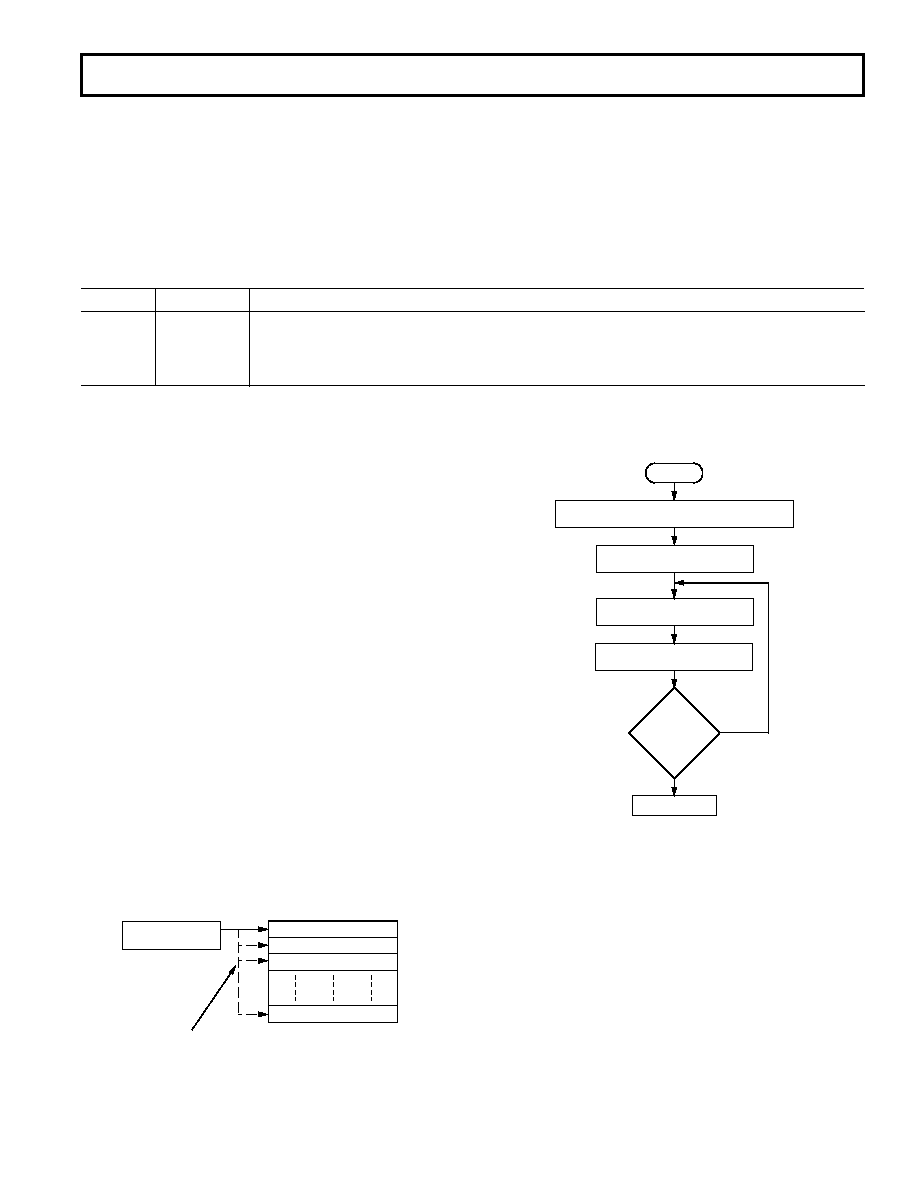
operation resets the calibration register pointer. The flowchart
in Figure 6 shows the sequence for writing to the calibration
registers. Figure 7 shows the sequence for reading from the cali-
bration registers.
CALIBRATION REGISTERS
GAIN REGISTER
OFFSET REGISTER
DAC 1ST MSB REGISTER
(1)
(2)
(3)
DAC 8TH MSB REGISTER
(10)
CAL REGISTER
ADDRESS POINTER
CALIBRATION REGISTER ADDRESS POINTER POSITION IS
DETERMINED BY THE NUMBER OF CALIBRATION REGISTERS
ADDRESSED AND THE NUMBER OF READ/WRITE OPERATIONS.
Figure 5. Calibration Register Arrangement
When reading from the calibration registers there are always two
leading zeros for each of the registers.
WRITE TO CONTROL REGISTER SETTING STCAL = 0
AND CALSLT1, CALSLT0 = 00, 01, 10, 11
START
CAL REGISTER POINTER IS
AUTOMATICALLY RESET
WRITE TO CAL REGISTER
(ADDR1 = 1, ADDR0 = 0)
CAL REGISTER POINTER IS
AUTOMATICALLY INCREMENTED
LAST
REGISTER
WRITE
OPERATION
OR
ABORT
?
FINISHED
NO
YES
Figure 6. Flowchart for Writing to the Calibration Registers
相关PDF资料 |
PDF描述 |
|---|---|
| VI-J14-MY-F4 | CONVERTER MOD DC/DC 48V 50W |
| VI-J13-MY-F4 | CONVERTER MOD DC/DC 24V 50W |
| AD7495BRMZ | IC ADC 12BIT SRL LP W/REF 8MSOP |
| AD7495BRZ | IC ADC 12BIT SRL LP W/REF 8-SOIC |
| UTS7124S | CONN RCPT 4X1.6 FEMALE JAM NUT |
相关代理商/技术参数 |
参数描述 |
|---|---|
| AD7854LARSZ-REEL | 功能描述:IC ADC 12BIT PARALLEL LP 28SSOP RoHS:是 类别:集成电路 (IC) >> 数据采集 - 模数转换器 系列:- 标准包装:1,000 系列:- 位数:16 采样率(每秒):45k 数据接口:串行 转换器数目:2 功率耗散(最大):315mW 电压电源:模拟和数字 工作温度:0°C ~ 70°C 安装类型:表面贴装 封装/外壳:28-SOIC(0.295",7.50mm 宽) 供应商设备封装:28-SOIC W 包装:带卷 (TR) 输入数目和类型:2 个单端,单极 |
| AD7854LARZ | 功能描述:IC ADC 12BIT PARALLEL LP 28-SOIC RoHS:是 类别:集成电路 (IC) >> 数据采集 - 模数转换器 系列:- 其它有关文件:TSA1204 View All Specifications 标准包装:1 系列:- 位数:12 采样率(每秒):20M 数据接口:并联 转换器数目:2 功率耗散(最大):155mW 电压电源:模拟和数字 工作温度:-40°C ~ 85°C 安装类型:表面贴装 封装/外壳:48-TQFP 供应商设备封装:48-TQFP(7x7) 包装:Digi-Reel® 输入数目和类型:4 个单端,单极;2 个差分,单极 产品目录页面:1156 (CN2011-ZH PDF) 其它名称:497-5435-6 |
| AD7854LARZ-REEL | 功能描述:IC ADC 12BIT PARALLEL LP 28SOIC RoHS:是 类别:集成电路 (IC) >> 数据采集 - 模数转换器 系列:- 标准包装:1,000 系列:- 位数:16 采样率(每秒):45k 数据接口:串行 转换器数目:2 功率耗散(最大):315mW 电压电源:模拟和数字 工作温度:0°C ~ 70°C 安装类型:表面贴装 封装/外壳:28-SOIC(0.295",7.50mm 宽) 供应商设备封装:28-SOIC W 包装:带卷 (TR) 输入数目和类型:2 个单端,单极 |
| AD7854LBR | 制造商:未知厂家 制造商全称:未知厂家 功能描述:Analog-to-Digital Converter, 12-Bit |
| AD7854SQ | 制造商:Rochester Electronics LLC 功能描述:12-BIT SINGLE CH.PARALLEL ADC I.C. - Bulk |
发布紧急采购,3分钟左右您将得到回复。