- 您现在的位置:买卖IC网 > PDF目录10541 > AD7854LARSZ (Analog Devices Inc)IC ADC 12BIT PARALLEL LP 28SSOP PDF资料下载
参数资料
| 型号: | AD7854LARSZ |
| 厂商: | Analog Devices Inc |
| 文件页数: | 27/28页 |
| 文件大小: | 0K |
| 描述: | IC ADC 12BIT PARALLEL LP 28SSOP |
| 标准包装: | 47 |
| 位数: | 12 |
| 采样率(每秒): | 100k |
| 数据接口: | 并联 |
| 转换器数目: | 2 |
| 功率耗散(最大): | 30mW |
| 电压电源: | 模拟和数字 |
| 工作温度: | -40°C ~ 85°C |
| 安装类型: | 表面贴装 |
| 封装/外壳: | 28-SSOP(0.209",5.30mm 宽) |
| 供应商设备封装: | 28-SSOP |
| 包装: | 管件 |
| 输入数目和类型: | 1 个伪差分,单极;1 个伪差分,双极 |
第1页第2页第3页第4页第5页第6页第7页第8页第9页第10页第11页第12页第13页第14页第15页第16页第17页第18页第19页第20页第21页第22页第23页第24页第25页第26页当前第27页第28页
AD7854/AD7854L
–8–
REV. B
AD7854/AD7854L ON-CHIP REGISTERS
The AD7854/AD7854L powers up with a set of default conditions, and the user need not ever write to the device. In this case the
AD7854/AD7854L will operate as a read-only ADC. The
WR pin should be tied to DV
DD for operating the AD7854/AD7854L as a
read-only ADC.
Extra features and flexibility such as performing different power-down options, different types of calibrations including system cali-
bration, and software conversion start can be selected by writing to the part.
The AD7854/AD7854L contains a control register, ADC output data register, status register, test register and 10 calibra-
tion registers. The control register is write-only, the ADC output data register and the status register are read-only, and the test and
calibration registers are both read/write registers. The test register is used for testing the part and should not be written to.
Addressing the On-Chip Registers
Writing
To write to the AD7854/AD7854L, a 16-bit word of data must be transferred. This transfer consists of two 8-bit writes. The first
8 bits of data that are written must consist of the 8 LSBs of the 16-bit word and the second 8 bits that are written must consist of the
8 MSBs of the 16-bit word. For each of these 8-bit writes, the data is placed on Pins DB0 to DB7, Pin DB0 being the LSB of each
transfer and Pin DB7 being the MSB of each transfer. The two MSBs of the 16-bit word, ADDR1 and ADDR0, are decoded to
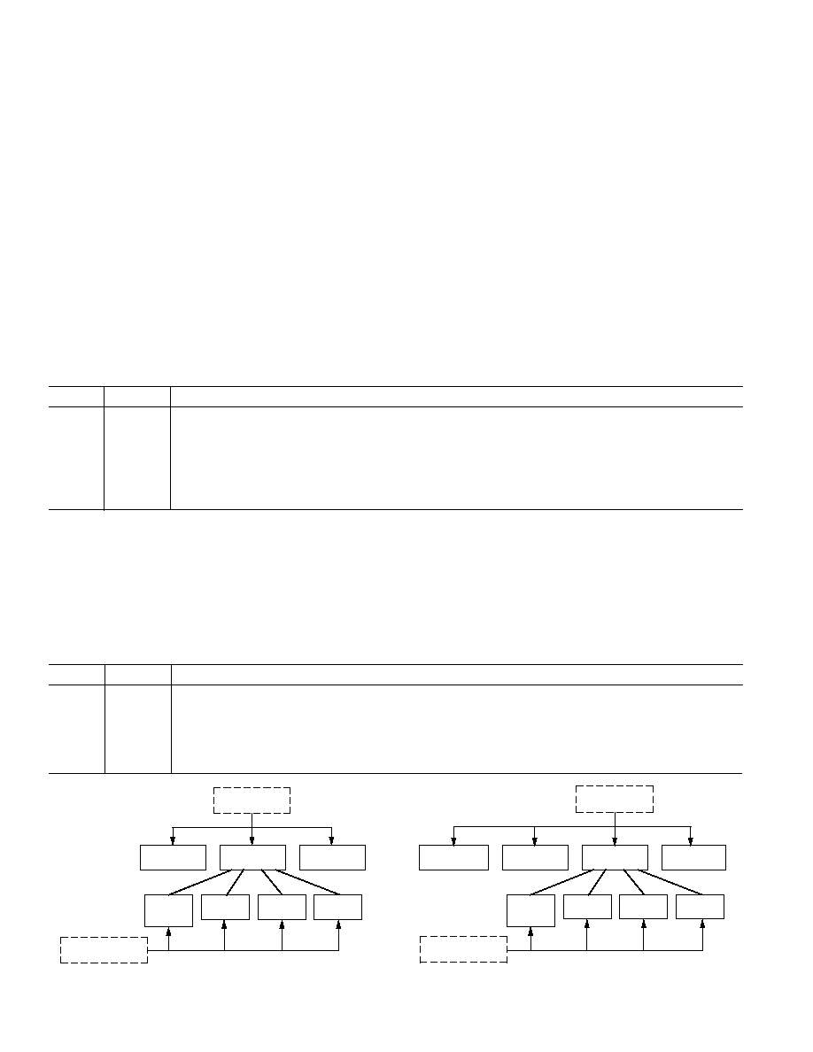
determine which register is addressed, and the 14 LSBs are written to the addressed register. Table I shows the decoding of the
address bits, while Figure 2 shows the overall write register hierarchy.
Table I. Write Register Addressing
ADDR1
ADDR0
Comment
0
This combination does not address any register.
0
1
This combination addresses the TEST REGISTER. The 14 LSBs of data are written to the test register.
1
0
This combination addresses the CALIBRATION REGISTER. The 14 least significant data bits are writ-
ten to the selected calibration register.
1
This combination addresses the CONTROL REGISTER. The 14 least significant data bits are written to
the control register.
Reading
To read from the various registers the user must first write to Bits 6 and 7 in the Control Register, RDSLT0 and RDSLT1. These
bits are decoded to determine which register is addressed during a read operation. Table II shows the decoding of the read address
bits while Figure 3 shows the overall read register hierarchy. The power-up status of these bits is 00 so that the default read will be
from the ADC output data register. Note: when reading from the calibration registers, the low byte must always be read first.
Once the read selection bits are set in the control register all subsequent read operations that follow are from the selected register
until the read selection bits are changed in the control register.
Table II. Read Register Addressing
RDSLT1
RDSLT0
Comment
0
All successive read operations are from the ADC OUTPUT DATA REGISTER. This is the default power-
up setting. There is always four leading zeros when reading from the ADC output data register.
0
1
All successive read operations are from the TEST REGISTER.
1
0
All successive read operations are from the CALIBRATION REGISTERS.
1
All successive read operations are from the STATUS REGISTER.
TEST
REGISTER
CALIBRATION
REGISTERS
CONTROL
REGISTER
ADDR1, ADDR0
DECODE
01
10
11
GAIN(1)
OFFSET(1)
DAC(8)
GAIN(1)
OFFSET(1)
GAIN(1)
CALSLT1, CALSLT0
DECODE
00
01
10
11
Figure 2. Write Register Hierarchy/Address Decoding
TEST
REGISTER
CALIBRATION
REGISTERS
CONTROL
REGISTER
RDSLT1, RDSLT0
DECODE
01
10
11
GAIN(1)
OFFSET(1)
DAC(8)
GAIN(1)
OFFSET(1)
GAIN(1)
CALSLT1, CALSLT0
DECODE
00
01
10
11
ADC OUTPUT
DATA REGISTER
00
Figure 3. Read Register Hierarchy/Address Decoding
相关PDF资料 |
PDF描述 |
|---|---|
| VI-J14-MY-F4 | CONVERTER MOD DC/DC 48V 50W |
| VI-J13-MY-F4 | CONVERTER MOD DC/DC 24V 50W |
| AD7495BRMZ | IC ADC 12BIT SRL LP W/REF 8MSOP |
| AD7495BRZ | IC ADC 12BIT SRL LP W/REF 8-SOIC |
| UTS7124S | CONN RCPT 4X1.6 FEMALE JAM NUT |
相关代理商/技术参数 |
参数描述 |
|---|---|
| AD7854LARSZ-REEL | 功能描述:IC ADC 12BIT PARALLEL LP 28SSOP RoHS:是 类别:集成电路 (IC) >> 数据采集 - 模数转换器 系列:- 标准包装:1,000 系列:- 位数:16 采样率(每秒):45k 数据接口:串行 转换器数目:2 功率耗散(最大):315mW 电压电源:模拟和数字 工作温度:0°C ~ 70°C 安装类型:表面贴装 封装/外壳:28-SOIC(0.295",7.50mm 宽) 供应商设备封装:28-SOIC W 包装:带卷 (TR) 输入数目和类型:2 个单端,单极 |
| AD7854LARZ | 功能描述:IC ADC 12BIT PARALLEL LP 28-SOIC RoHS:是 类别:集成电路 (IC) >> 数据采集 - 模数转换器 系列:- 其它有关文件:TSA1204 View All Specifications 标准包装:1 系列:- 位数:12 采样率(每秒):20M 数据接口:并联 转换器数目:2 功率耗散(最大):155mW 电压电源:模拟和数字 工作温度:-40°C ~ 85°C 安装类型:表面贴装 封装/外壳:48-TQFP 供应商设备封装:48-TQFP(7x7) 包装:Digi-Reel® 输入数目和类型:4 个单端,单极;2 个差分,单极 产品目录页面:1156 (CN2011-ZH PDF) 其它名称:497-5435-6 |
| AD7854LARZ-REEL | 功能描述:IC ADC 12BIT PARALLEL LP 28SOIC RoHS:是 类别:集成电路 (IC) >> 数据采集 - 模数转换器 系列:- 标准包装:1,000 系列:- 位数:16 采样率(每秒):45k 数据接口:串行 转换器数目:2 功率耗散(最大):315mW 电压电源:模拟和数字 工作温度:0°C ~ 70°C 安装类型:表面贴装 封装/外壳:28-SOIC(0.295",7.50mm 宽) 供应商设备封装:28-SOIC W 包装:带卷 (TR) 输入数目和类型:2 个单端,单极 |
| AD7854LBR | 制造商:未知厂家 制造商全称:未知厂家 功能描述:Analog-to-Digital Converter, 12-Bit |
| AD7854SQ | 制造商:Rochester Electronics LLC 功能描述:12-BIT SINGLE CH.PARALLEL ADC I.C. - Bulk |
发布紧急采购,3分钟左右您将得到回复。