- 您现在的位置:买卖IC网 > PDF目录10541 > AD7854LARSZ (Analog Devices Inc)IC ADC 12BIT PARALLEL LP 28SSOP PDF资料下载
参数资料
| 型号: | AD7854LARSZ |
| 厂商: | Analog Devices Inc |
| 文件页数: | 6/28页 |
| 文件大小: | 0K |
| 描述: | IC ADC 12BIT PARALLEL LP 28SSOP |
| 标准包装: | 47 |
| 位数: | 12 |
| 采样率(每秒): | 100k |
| 数据接口: | 并联 |
| 转换器数目: | 2 |
| 功率耗散(最大): | 30mW |
| 电压电源: | 模拟和数字 |
| 工作温度: | -40°C ~ 85°C |
| 安装类型: | 表面贴装 |
| 封装/外壳: | 28-SSOP(0.209",5.30mm 宽) |
| 供应商设备封装: | 28-SSOP |
| 包装: | 管件 |
| 输入数目和类型: | 1 个伪差分,单极;1 个伪差分,双极 |
第1页第2页第3页第4页第5页当前第6页第7页第8页第9页第10页第11页第12页第13页第14页第15页第16页第17页第18页第19页第20页第21页第22页第23页第24页第25页第26页第27页第28页
AD7854/AD7854L
–14–
REV. B
INPUT FREQUENCY – kHz
–72
–92
0
100
20
THD
–
dB
40
60
80
–76
–80
–84
–88
RIN = 1k
RIN = 50 , 10nF
AS IN FIGURE 13
THD VS. FREQUENCY FOR DIFFERENT
SOURCE IMPEDANCES
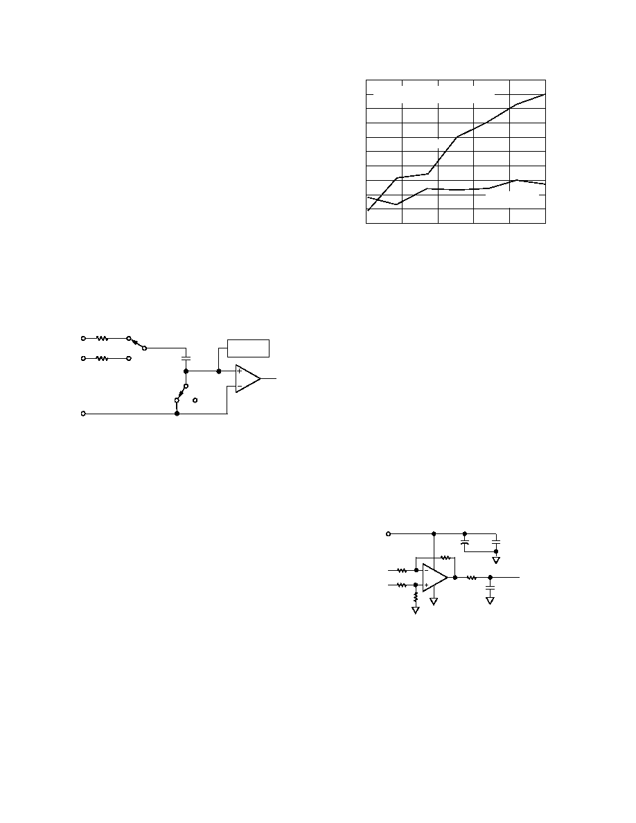
Figure 10. THD vs. Analog Input Frequency
The maximum source impedance depends on the amount of
total harmonic distortion (THD) that can be tolerated. The
THD increases as the source impedance increases. Figure 10
shows a graph of the total harmonic distortion vs. analog input
signal frequency for different source impedances. With the
setup as in Figure 11, the THD is at the –90 dB level. With a
source impedance of 1 k
and no capacitor on the AIN(+) pin,
the THD increases with frequency.
In a single supply application (both 3 V and 5 V), the V+ and
V– of the op amp can be taken directly from the supplies to the
AD7854/AD7854L which eliminates the need for extra external
power supplies. When operating with rail-to-rail inputs and out-
puts at frequencies greater than 10 kHz, care must be taken in
selecting the particular op amp for the application. In particular,
for single supply applications the input amplifiers should be
connected in a gain of –1 arrangement to get the optimum per-
formance. Figure 11 shows the arrangement for a single supply
application with a 50
and 10 nF low-pass filter (cutoff fre-
quency 320 kHz) on the AIN(+) pin. Note that the 10 nF is a
capacitor with good linearity to ensure good ac performance.
Recommended single supply op amps are the AD820 and the
AD820-3V.
V–
V+
10k
VIN
(–VREF/2 TO +VREF/2)
VREF/2
0.1 F
10 F
50
10nF
(NPO)
AD820
AD820-3V
TO AIN(+) OF
AD7854/AD7854L
+3V TO +5V
10k
IC1
10k
Figure 11. Analog Input Buffering
ANALOG INPUT
The equivalent analog input circuit is shown in Figure 9. Dur-
ing the acquisition interval the switches are both in the track
position and the AIN(+) charges the 20 pF capacitor through
the 125
resistance. On the rising edge of CONVST switches
SW1 and SW2 go into the hold position retaining charge on the
20 pF capacitor as a sample of the signal on AIN(+). The
AIN(–) is connected to the 20 pF capacitor, and this unbalances
the voltage at Node A at the input of the comparator. The
capacitor DAC adjusts during the remainder of the conversion
cycle to restore the voltage at Node A to the correct value. This
action transfers a charge, representing the analog input signal, to
the capacitor DAC which in turn forms a digital representation
of the analog input signal. The voltage on the AIN(–) pin directly
influences the charge transferred to the capacitor DAC at the
hold instant. If this voltage changes during the conversion period,
the DAC representation of the analog input voltage is altered.
Therefore it is most important that the voltage on the AIN(–)
pin remains constant during the conversion period. Further-
more, it is recommended that the AIN(–) pin is always connected
to AGND or to a fixed dc voltage.
CAPACITOR
DAC
COMPARATOR
20pF
HOLD
TRACK
SW2
TRACK
SW1
HOLD
125
AIN(+)
125
AIN(–)
AGND
NODE A
Figure 9. Analog Input Equivalent Circuit
Acquisition Time
The track-and-hold amplifier enters its tracking mode on the
falling edge of the BUSY signal. The time required for the
track-and-hold amplifier to acquire an input signal depends on
how quickly the 20 pF input capacitance is charged. There is a
minimum acquisition time of 400 ns. For large source imped-
ances, >2 k
, the acquisition time is calculated using the formula:
tACQ = 9
× (RIN + 125 ) × 20 pF
where RIN is the source impedance of the input signal, and
125
, 20 pF is the input R, C.
DC/AC Applications
For dc applications, high source impedances are acceptable,
provided there is enough acquisition time between conversions
to charge the 20 pF capacitor. For example with RIN = 5 k
,
the required acquisition time is 922 ns.
For ac applications, removing high frequency components from
the analog input signal is recommended by use of an RC low-
pass filter on the AIN(+) pin, as shown in Figure 11. In applica-
tions where harmonic distortion and signal to noise ratio are
critical, the analog input should be driven from a low impedance
source. Large source impedances significantly affect the ac per-
formance of the ADC. They may require the use of an input
buffer amplifier. The choice of the amplifier is a function of the
particular application.
相关PDF资料 |
PDF描述 |
|---|---|
| VI-J14-MY-F4 | CONVERTER MOD DC/DC 48V 50W |
| VI-J13-MY-F4 | CONVERTER MOD DC/DC 24V 50W |
| AD7495BRMZ | IC ADC 12BIT SRL LP W/REF 8MSOP |
| AD7495BRZ | IC ADC 12BIT SRL LP W/REF 8-SOIC |
| UTS7124S | CONN RCPT 4X1.6 FEMALE JAM NUT |
相关代理商/技术参数 |
参数描述 |
|---|---|
| AD7854LARSZ-REEL | 功能描述:IC ADC 12BIT PARALLEL LP 28SSOP RoHS:是 类别:集成电路 (IC) >> 数据采集 - 模数转换器 系列:- 标准包装:1,000 系列:- 位数:16 采样率(每秒):45k 数据接口:串行 转换器数目:2 功率耗散(最大):315mW 电压电源:模拟和数字 工作温度:0°C ~ 70°C 安装类型:表面贴装 封装/外壳:28-SOIC(0.295",7.50mm 宽) 供应商设备封装:28-SOIC W 包装:带卷 (TR) 输入数目和类型:2 个单端,单极 |
| AD7854LARZ | 功能描述:IC ADC 12BIT PARALLEL LP 28-SOIC RoHS:是 类别:集成电路 (IC) >> 数据采集 - 模数转换器 系列:- 其它有关文件:TSA1204 View All Specifications 标准包装:1 系列:- 位数:12 采样率(每秒):20M 数据接口:并联 转换器数目:2 功率耗散(最大):155mW 电压电源:模拟和数字 工作温度:-40°C ~ 85°C 安装类型:表面贴装 封装/外壳:48-TQFP 供应商设备封装:48-TQFP(7x7) 包装:Digi-Reel® 输入数目和类型:4 个单端,单极;2 个差分,单极 产品目录页面:1156 (CN2011-ZH PDF) 其它名称:497-5435-6 |
| AD7854LARZ-REEL | 功能描述:IC ADC 12BIT PARALLEL LP 28SOIC RoHS:是 类别:集成电路 (IC) >> 数据采集 - 模数转换器 系列:- 标准包装:1,000 系列:- 位数:16 采样率(每秒):45k 数据接口:串行 转换器数目:2 功率耗散(最大):315mW 电压电源:模拟和数字 工作温度:0°C ~ 70°C 安装类型:表面贴装 封装/外壳:28-SOIC(0.295",7.50mm 宽) 供应商设备封装:28-SOIC W 包装:带卷 (TR) 输入数目和类型:2 个单端,单极 |
| AD7854LBR | 制造商:未知厂家 制造商全称:未知厂家 功能描述:Analog-to-Digital Converter, 12-Bit |
| AD7854SQ | 制造商:Rochester Electronics LLC 功能描述:12-BIT SINGLE CH.PARALLEL ADC I.C. - Bulk |
发布紧急采购,3分钟左右您将得到回复。