- 您现在的位置:买卖IC网 > PDF目录17099 > AD9148-EBZ (Analog Devices Inc)BOARD EVALUATION FOR AD9148 PDF资料下载
参数资料
| 型号: | AD9148-EBZ |
| 厂商: | Analog Devices Inc |
| 文件页数: | 36/72页 |
| 文件大小: | 0K |
| 描述: | BOARD EVALUATION FOR AD9148 |
| 设计资源: | AD9148-EBZ Schematic AD9148-EBZ BOM AD9148-EBZ Gerber Files |
| 标准包装: | 1 |
| 系列: | TxDAC+® |
| DAC 的数量: | 4 |
| 位数: | 16 |
| 采样率(每秒): | 1G |
| 数据接口: | 串行,SPI? |
| 设置时间: | 20ns |
| DAC 型: | 电流 |
| 工作温度: | -40°C ~ 85°C |
| 已供物品: | 板 |
| 已用 IC / 零件: | AD9148 |
第1页第2页第3页第4页第5页第6页第7页第8页第9页第10页第11页第12页第13页第14页第15页第16页第17页第18页第19页第20页第21页第22页第23页第24页第25页第26页第27页第28页第29页第30页第31页第32页第33页第34页第35页当前第36页第37页第38页第39页第40页第41页第42页第43页第44页第45页第46页第47页第48页第49页第50页第51页第52页第53页第54页第55页第56页第57页第58页第59页第60页第61页第62页第63页第64页第65页第66页第67页第68页第69页第70页第71页第72页
Data Sheet
AD9148
Rev. B | Page 41 of 72
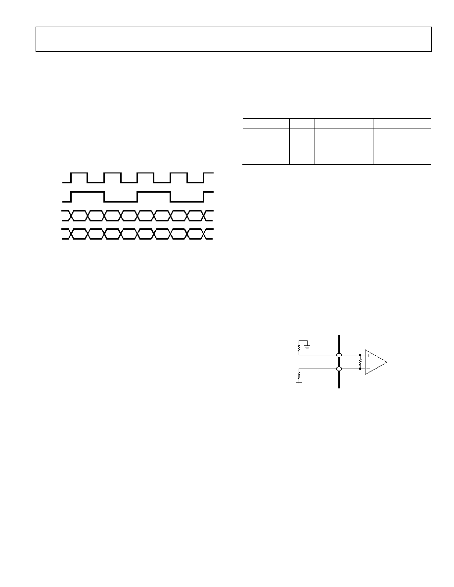
BYTE MODE
In byte mode, a FRAME signal must be provided along with the
DCI signal and the data. The most significant byte of the data
should correspond with DCI being high, and the least significant
byte of the data should correspond with DCI being low. The
FRAME signal indicates to which DAC the data is intended.
When FRAME is high, data on the top half of the port (A[15:8])
is sent to DAC 1 and data on the bottom half of the port (A[7:0]) is
sent to DAC 3. When the FRAME is low, data on the top half of
the port is sent to DAC 2 and data on the bottom half of the port
is sent to DAC 4. This pattern repeats continuously as shown in
FRAMEA
A[15:8]
DAC1H
DAC1L
DAC2H
DAC2L
DAC1H
DAC1L
DAC2H
DAC2L
A[7:0]
DAC3H
DAC3L
DAC4H
DAC4L
DAC3H
DAC3L
DAC4H
DAC4L
DCIA
08910-
048
Figure 48. Timing Diagram for Byte Mode
The AD9148 also includes a byte swap feature. By default, the
bytes should be formatted as an MSB sent to Bit 15 on Bus 1 and
Bit 7 on Bus 2. When byte swap is enabled (Register 0x03[2]), an
MSB should be sent to Bit 8 on Bus 1 and Bit 0 on Bus 2. This
is described in Table 14.
Table 14. Byte Swap Formatting
Byte Swap
Byte
A[15:8]
A[7:0]
0
MSB
Data Set 1[15:8]
Data Set 2[15:8]
0
LSB
Data Set 1[7:0]
Data Set 2[7:0]
1
MSB
Data Set 1[8:15]
Data Set 2[8:15]
1
LSB
Data Set 1[0:7]
Data Set 2[0:7]
DATA INTERFACE OPTIONS
To enable optimization of the data interface, some additional
options have been provided in the following registers:
Data format (Register 0x03)
Data receiver control (Register 0x14)
Data receiver status (Register 0x15)
Depending on the data rate and DCI vs. data skew, the internal
DCI can be inverted to meet the valid data timing window.
RECOMMENDED FRAME INPUT BIAS CIRCUITRY
Because the frame signal can be used as a reference clock in the
byte mode or as a trigger to reset the FIFO, it is recommended
that the frame input be tied to LVDS logic low when it is not
used (that is, when it is not driven by an ASIC or FPGA). The
external bias circuit shown in Figure 49 is recommended for
this purpose. This bias circuit applies to both FRAMEA and
FRAMEB ports.
08910-
145
100
150
51
AD9148
FRAMEP
FRAMEN
DVDD18
(1.8V)
Figure 49. External Bias Circuit
相关PDF资料 |
PDF描述 |
|---|---|
| SCRH124-150 | INDUCTOR SMD 15UH 3.20A 100KHZ |
| SCRH6D28-470 | INDUCTOR SMD 47UH 0.80A 10KHZ |
| 0982660828 | CBL 13POS 0.5MM JMPR TYPE D 10" |
| HCM12DSEN-S243 | CONN EDGECARD 24POS .156 EYELET |
| RBM12DCAD | CONN EDGECARD 24POS R/A .156 SLD |
相关代理商/技术参数 |
参数描述 |
|---|---|
| AD9148-M5372-EBZ | 功能描述:BOARD EVAL FOR AD9149, ADL5372 RoHS:是 类别:编程器,开发系统 >> 评估板 - 数模转换器 (DAC) 系列:* 产品培训模块:Lead (SnPb) Finish for COTS Obsolescence Mitigation Program 标准包装:1 系列:- DAC 的数量:4 位数:12 采样率(每秒):- 数据接口:串行,SPI? 设置时间:3µs DAC 型:电流/电压 工作温度:-40°C ~ 85°C 已供物品:板 已用 IC / 零件:MAX5581 |
| AD9148-M5375-EBZ | 功能描述:BOARD EVAL FOR AD9149, ADL5375 RoHS:是 类别:编程器,开发系统 >> 评估板 - 数模转换器 (DAC) 系列:* 产品培训模块:Lead (SnPb) Finish for COTS Obsolescence Mitigation Program 标准包装:1 系列:- DAC 的数量:4 位数:12 采样率(每秒):- 数据接口:串行,SPI? 设置时间:3µs DAC 型:电流/电压 工作温度:-40°C ~ 85°C 已供物品:板 已用 IC / 零件:MAX5581 |
| AD9152BCPZ | 功能描述:16 Bit Digital to Analog Converter 2 56-LFCSP-WQ (8x8) 制造商:analog devices inc. 系列:TxDAC+? 包装:托盘 零件状态:有效 位数:16 数模转换器数:2 建立时间:- 输出类型:Current - Unbuffered 差分输出:是 数据接口:JESD204B 参考类型:内部 电压 - 电源,模拟:3.13 V ~ 3.47 V 电压 - 电源,数字:1.14 V ~ 1.26 V INL/DNL(LSB):±10,±5 架构:电流源 工作温度:-40°C ~ 85°C 封装/外壳:56-WFQFN 裸焊盘,CSP 供应商器件封装:56-LFCSP-WQ(8x8) 标准包装:1 |
| AD9152BCPZRL | 功能描述:16 Bit Digital to Analog Converter 2 56-LFCSP-WQ (8x8) 制造商:analog devices inc. 系列:TxDAC+? 包装:带卷(TR) 零件状态:有效 位数:16 数模转换器数:2 建立时间:- 输出类型:Current - Unbuffered 差分输出:是 数据接口:JESD204B 参考类型:内部 电压 - 电源,模拟:3.13 V ~ 3.47 V 电压 - 电源,数字:1.14 V ~ 1.26 V INL/DNL(LSB):±10,±5 架构:电流源 工作温度:-40°C ~ 85°C 封装/外壳:56-WFQFN 裸焊盘,CSP 供应商器件封装:56-LFCSP-WQ(8x8) 标准包装:2,500 |
| AD9152-EBZ | 功能描述:AD9152 TxDAC+? Series 16 Bit 2.25G Samples Per Second Digital to Analog Converter (DAC) Evaluation Board 制造商:analog devices inc. 系列:TxDAC+? 零件状态:有效 DAC 数:2 位数:16 采样率(每秒):2.25G 数据接口:SPI 建立时间:- DAC 类型:电流 工作温度:-40°C ~ 85°C 所含物品:板,线缆 使用的 IC/零件:AD9152 标准包装:1 |
发布紧急采购,3分钟左右您将得到回复。