- 您现在的位置:买卖IC网 > PDF目录17099 > AD9148-EBZ (Analog Devices Inc)BOARD EVALUATION FOR AD9148 PDF资料下载
参数资料
| 型号: | AD9148-EBZ |
| 厂商: | Analog Devices Inc |
| 文件页数: | 37/72页 |
| 文件大小: | 0K |
| 描述: | BOARD EVALUATION FOR AD9148 |
| 设计资源: | AD9148-EBZ Schematic AD9148-EBZ BOM AD9148-EBZ Gerber Files |
| 标准包装: | 1 |
| 系列: | TxDAC+® |
| DAC 的数量: | 4 |
| 位数: | 16 |
| 采样率(每秒): | 1G |
| 数据接口: | 串行,SPI? |
| 设置时间: | 20ns |
| DAC 型: | 电流 |
| 工作温度: | -40°C ~ 85°C |
| 已供物品: | 板 |
| 已用 IC / 零件: | AD9148 |
第1页第2页第3页第4页第5页第6页第7页第8页第9页第10页第11页第12页第13页第14页第15页第16页第17页第18页第19页第20页第21页第22页第23页第24页第25页第26页第27页第28页第29页第30页第31页第32页第33页第34页第35页第36页当前第37页第38页第39页第40页第41页第42页第43页第44页第45页第46页第47页第48页第49页第50页第51页第52页第53页第54页第55页第56页第57页第58页第59页第60页第61页第62页第63页第64页第65页第66页第67页第68页第69页第70页第71页第72页
AD9148
Data Sheet
Rev. B | Page 42 of 72
FIFO OPERATION
DAC1
AND
DAC2
32
32 BITS
÷INT
DCIA
DCIB
DACCLK
DATA
PORT A
DATA
PORT B
DATA
PATHS
DATA
ASSEMBLER
INPUT
LATCH
DATA
ASSEMBLER
INPUT
LATCH
REG 0
REG 1
REG 2
REG 3
REG 4
REG 5
REG 6
REG 7
REG 0
REG 1
REG 2
REG 3
REG 4
REG 5
REG 6
REG 7
32
DAC3
AND
DAC4
32
DATA
PATHS
32
WRITE PTR
RESET
WRITE PTR
RESET
READ
PTR
RESET
SYNC
LOGIC
FIFO RATE/
DATA RATE
FI
F
O
A
O
F
S
[2:
0]
FI
F
O
B
OF
S
[2
:0
]
32 BITS
FRAMEB
FRAMEA
LOGIC
RE
AD
P
O
IN
T
E
R
A
R
E
AD
P
O
INT
E
R
B
32
INTERFACE
MODE
ONE
DCI
WRITE PTR B
WRITE PTR A
08
91
0-
049
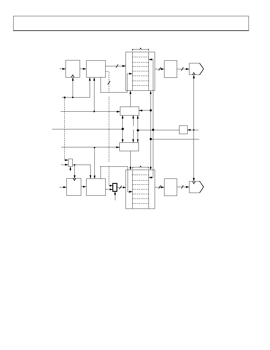
Figure 50. Block Diagram of FIFO
The AD9148 contains two 32-bit wide, 8-word deep FIFOs (one
per dual DAC) designed to relax the timing relationship between
the data arriving at the DAC input ports and the internal DAC
data rate clock. The FIFOs can also be used to provide an adjustable
pipeline delay between the DCIx clocks and the DACCLK allowing
realignment of data input in a multichip system. This significantly
increases the timing budget of the interface.
Figure 50 shows the block diagram of the datapath through the
FIFO. The data is latched into the device, is formatted, and is then
written into the FIFO register determined by the FIFO write
pointer. The value of the write pointer is incremented every time a
new word is loaded into the FIFO. Meanwhile, data is read from
the FIFO register determined by the read pointer and fed into
the digital datapath. The value of the read pointer is updated
every time data is read into the datapath from the FIFO. This
happens at the data rate, that is, the DACCLK rate divided by
the interpolation ratio. The difference between the write and
read pointers represents the FIFO pipeline delay and is
important to take into account when understanding the overall
pipeline delay of the AD9148.
In single-port and byte interface modes, the incoming digital data is
sampled at twice the data rate (DCIA). The data is then assembled
based on the interface mode. At the output of the data assembler
block, the data samples for DAC 1 and DAC 2 are written to FIFO A
and the data samples for DAC 3 and DAC 4 are written to FIFO B
at the data rate.
Valid data is transmitted through the FIFO as long as the FIFO
does not overflow or become empty. An overflow or empty
condition of the FIFO is the same as the write pointer and the
read pointer being equal. When both pointers are equal, an attempt
is made to read and write a single FIFO register simultaneously.
This simultaneous register access leads to unreliable data transfer
through the FIFO and must be avoided.
相关PDF资料 |
PDF描述 |
|---|---|
| SCRH124-150 | INDUCTOR SMD 15UH 3.20A 100KHZ |
| SCRH6D28-470 | INDUCTOR SMD 47UH 0.80A 10KHZ |
| 0982660828 | CBL 13POS 0.5MM JMPR TYPE D 10" |
| HCM12DSEN-S243 | CONN EDGECARD 24POS .156 EYELET |
| RBM12DCAD | CONN EDGECARD 24POS R/A .156 SLD |
相关代理商/技术参数 |
参数描述 |
|---|---|
| AD9148-M5372-EBZ | 功能描述:BOARD EVAL FOR AD9149, ADL5372 RoHS:是 类别:编程器,开发系统 >> 评估板 - 数模转换器 (DAC) 系列:* 产品培训模块:Lead (SnPb) Finish for COTS Obsolescence Mitigation Program 标准包装:1 系列:- DAC 的数量:4 位数:12 采样率(每秒):- 数据接口:串行,SPI? 设置时间:3µs DAC 型:电流/电压 工作温度:-40°C ~ 85°C 已供物品:板 已用 IC / 零件:MAX5581 |
| AD9148-M5375-EBZ | 功能描述:BOARD EVAL FOR AD9149, ADL5375 RoHS:是 类别:编程器,开发系统 >> 评估板 - 数模转换器 (DAC) 系列:* 产品培训模块:Lead (SnPb) Finish for COTS Obsolescence Mitigation Program 标准包装:1 系列:- DAC 的数量:4 位数:12 采样率(每秒):- 数据接口:串行,SPI? 设置时间:3µs DAC 型:电流/电压 工作温度:-40°C ~ 85°C 已供物品:板 已用 IC / 零件:MAX5581 |
| AD9152BCPZ | 功能描述:16 Bit Digital to Analog Converter 2 56-LFCSP-WQ (8x8) 制造商:analog devices inc. 系列:TxDAC+? 包装:托盘 零件状态:有效 位数:16 数模转换器数:2 建立时间:- 输出类型:Current - Unbuffered 差分输出:是 数据接口:JESD204B 参考类型:内部 电压 - 电源,模拟:3.13 V ~ 3.47 V 电压 - 电源,数字:1.14 V ~ 1.26 V INL/DNL(LSB):±10,±5 架构:电流源 工作温度:-40°C ~ 85°C 封装/外壳:56-WFQFN 裸焊盘,CSP 供应商器件封装:56-LFCSP-WQ(8x8) 标准包装:1 |
| AD9152BCPZRL | 功能描述:16 Bit Digital to Analog Converter 2 56-LFCSP-WQ (8x8) 制造商:analog devices inc. 系列:TxDAC+? 包装:带卷(TR) 零件状态:有效 位数:16 数模转换器数:2 建立时间:- 输出类型:Current - Unbuffered 差分输出:是 数据接口:JESD204B 参考类型:内部 电压 - 电源,模拟:3.13 V ~ 3.47 V 电压 - 电源,数字:1.14 V ~ 1.26 V INL/DNL(LSB):±10,±5 架构:电流源 工作温度:-40°C ~ 85°C 封装/外壳:56-WFQFN 裸焊盘,CSP 供应商器件封装:56-LFCSP-WQ(8x8) 标准包装:2,500 |
| AD9152-EBZ | 功能描述:AD9152 TxDAC+? Series 16 Bit 2.25G Samples Per Second Digital to Analog Converter (DAC) Evaluation Board 制造商:analog devices inc. 系列:TxDAC+? 零件状态:有效 DAC 数:2 位数:16 采样率(每秒):2.25G 数据接口:SPI 建立时间:- DAC 类型:电流 工作温度:-40°C ~ 85°C 所含物品:板,线缆 使用的 IC/零件:AD9152 标准包装:1 |
发布紧急采购,3分钟左右您将得到回复。