- 您现在的位置:买卖IC网 > PDF目录10115 > AD9233BCPZRL7-105 (Analog Devices Inc)IC ADC 12BIT 105MSPS 48-LFCSP PDF资料下载
参数资料
| 型号: | AD9233BCPZRL7-105 |
| 厂商: | Analog Devices Inc |
| 文件页数: | 11/44页 |
| 文件大小: | 0K |
| 描述: | IC ADC 12BIT 105MSPS 48-LFCSP |
| 标准包装: | 750 |
| 位数: | 12 |
| 采样率(每秒): | 105M |
| 数据接口: | 串行,SPI? |
| 转换器数目: | 1 |
| 功率耗散(最大): | 350mW |
| 电压电源: | 单电源 |
| 工作温度: | -40°C ~ 85°C |
| 安装类型: | 表面贴装 |
| 封装/外壳: | 48-VFQFN 裸露焊盘,CSP |
| 供应商设备封装: | 48-LFCSP-VQ(7x7) |
| 包装: | 带卷 (TR) |
| 输入数目和类型: | 2 个单端,单极;1 个差分,单极 |
| 配用: | AD9233-125EBZ-ND - BOARD EVALUATION FOR AD9233 |
第1页第2页第3页第4页第5页第6页第7页第8页第9页第10页当前第11页第12页第13页第14页第15页第16页第17页第18页第19页第20页第21页第22页第23页第24页第25页第26页第27页第28页第29页第30页第31页第32页第33页第34页第35页第36页第37页第38页第39页第40页第41页第42页第43页第44页
AD9233
Rev. A | Page 19 of 44
A third option is to ac-couple a differential LVDS signal to the
sample clock input pins, as shown in Figure 48. The AD9510/
drivers offers excellent jitter performance.
054
92
-050
100
0.1F
50*
LVDS DRIVER
50*
CLK
*50 RESISTORS ARE OPTIONAL
CLK–
CLK+
ADC
AD9233
CLOCK
INPUT
CLOCK
INPUT
AD951x
Figure 48. Differential LVDS Sample Clock
In some applications, it is acceptable to drive the sample clock
inputs with a single-ended CMOS signal. In such applications,
directly drive CLK+ from a CMOS gate, while bypassing the
CLK pin to ground with a 0.1 μF capacitor. Although the
CLK+ input circuit supply is AVDD (1.8 V), this input is
designed to withstand input voltages up to 3.6 V, making the
selection of the drive logic voltage very flexible. When driving
CLK+ with a 1.8 V CMOS signal, it is required to bias the
CLK pin with a 0.1 μF capacitor in parallel with a 39 kΩ
resistor (see Figure 49). The 39 kΩ resistor is not required when
driving CLK+ with a 3.3 V CMOS signal (see Figure 50).
0549
2-
05
1
CLOCK
INPUT
0.1F
39k
AD951x
CMOS DRIVER
50*
OPTIONAL
100
*50 RESISTOR IS OPTIONAL
CLK–
CLK+
ADC
AD9233
VCC
1k
Figure 49. Single-Ended 1.8 V CMOS Sample Clock
054
92-
052
CLOCK
INPUT
0.1F
VCC
AD951x
CMOS DRIVER
50*
OPTIONAL
100
*50 RESISTOR IS OPTIONAL
CLK–
CLK+
ADC
AD9233
1k
Figure 50. Single-Ended 3.3 V CMOS Sample Clock
Clock Duty Cycle
Typical high speed ADCs use both clock edges to generate a
variety of internal timing signals. As a result, these ADCs may
be sensitive to clock duty cycle. Commonly, a ±5% tolerance is
required on the clock duty cycle to maintain dynamic perform-
ance characteristics.
The AD9233 contains a DCS that retimes the nonsampling, or
falling edge, providing an internal clock signal with a nominal
50% duty cycle. This allows a wide range of clock input duty
cycles without affecting the performance of the AD9233. Noise
and distortion performance are nearly flat for a wide range of
duty cycles when the DCS is on, as shown in Figure 31.
Jitter in the rising edge of the input is still of paramount
concern and is not reduced by the internal stabilization circuit.
The duty cycle control loop does not function for clock rates
less than 20 MHz nominally. The loop has a time constant
associated with it that needs to be considered in applications
where the clock rate can change dynamically, which requires a
wait time of 1.5 μs to 5 μs after a dynamic clock frequency
increase (or decrease) before the DCS loop is relocked to the
input signal. During the time the loop is not locked, the DCS
loop is bypassed, and the internal device timing is dependant
on the duty cycle of the input clock signal. In such an application,
it can be appropriate to disable the duty cycle stabilizer. In all
other applications, enabling the DCS circuit is recommended to
maximize ac performance.
The DCS can be enabled or disabled by setting the SDIO/DCS
pin when operating in the external pin mode (see Table 10), or
via the SPI, as described in the Table 15.
Table 10. Mode Selection (External Pin Mode)
Voltage at Pin
SCLK/DFS
SDIO/DCS
AGND
Binary (default)
DCS disabled
AVDD
Twos complement
DCS enabled (default)
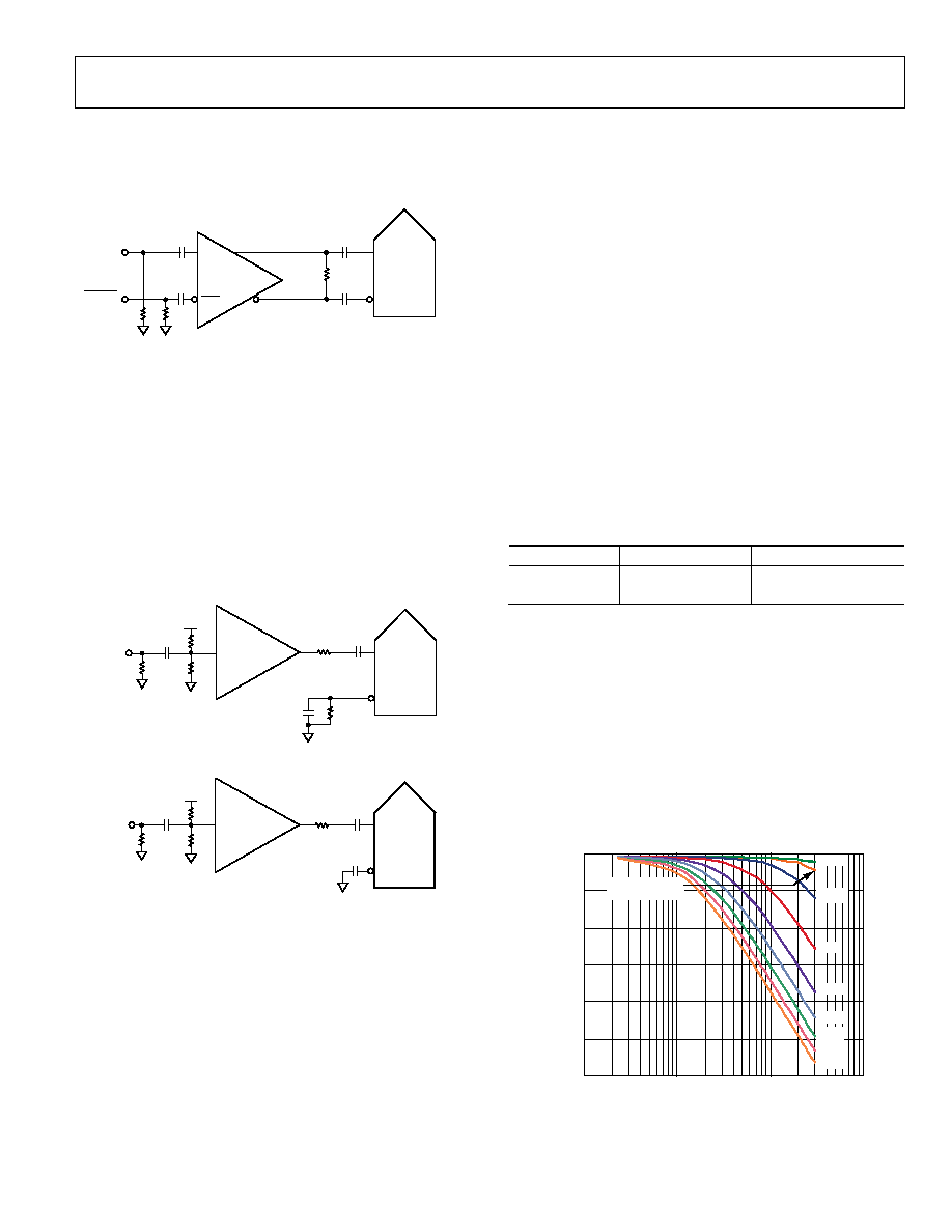
JITTER CONSIDERATIONS
High speed, high resolution ADCs are sensitive to the quality of
the clock input. The degradation in SNR at a given input
frequency (FIN) due to jitter (tJ) is calculated as
SNR = 20 log (2π × FIN × tJ)
In the equation, the rms aperture jitter (tJ) represents the root-
mean-square of all jitter sources, which include the clock input,
analog input signal, and ADC aperture jitter specification. IF
undersampling applications are particularly sensitive to jitter, as
shown in Figure 51.
70
65
60
55
50
45
40
1
10
100
1000
05
49
2-
04
6
S
NR
(
d
Bc)
INPUT FREQUENCY (MHz)
3.00ps
0.05ps
MEASURED
PERFORMANCE
0.20ps
0.5ps
1.0ps
1.50ps
2.00ps
2.50ps
Figure 51. SNR vs. Input Frequency and Jitter
相关PDF资料 |
PDF描述 |
|---|---|
| IDT72221L25J8 | IC FIFO SYNC 1KX9 25NS 32PLCC |
| MS27484T16A26PA | CONN PLUG 26POS STRAIGHT W/PINS |
| MS3476W14-12P | CONN PLUG 12POS STRAIGHT W/PINS |
| IDT72215LB25PF8 | IC FIFO 512X18 SYNC 25NS 64-TQFP |
| MS27473E16F35PB | CONN PLUG 55POS STRAIGHT W/PINS |
相关代理商/技术参数 |
参数描述 |
|---|---|
| AD9233BCPZRL7-125 | 功能描述:IC ADC 12BIT 125MSPS 48-LFCSP RoHS:是 类别:集成电路 (IC) >> 数据采集 - 模数转换器 系列:- 标准包装:1 系列:- 位数:14 采样率(每秒):83k 数据接口:串行,并联 转换器数目:1 功率耗散(最大):95mW 电压电源:双 ± 工作温度:0°C ~ 70°C 安装类型:通孔 封装/外壳:28-DIP(0.600",15.24mm) 供应商设备封装:28-PDIP 包装:管件 输入数目和类型:1 个单端,双极 |
| AD9233BCPZRL7-80 | 制造商:AD 制造商全称:Analog Devices 功能描述:12-Bit, 80 MSPS/105 MSPS/125 MSPS, 1.8 V Analog-to-Digital Converter |
| AD9234-1000EBZ | 功能描述:AD9234 - 12 Bit 1G Samples per Second Analog to Digital Converter (ADC) Evaluation Board 制造商:analog devices inc. 系列:- 零件状态:有效 A/D 转换器数:2 位数:12 采样率(每秒):1G 数据接口:JESD204B 输入范围:1.34 Vpp 不同条件下的功率(典型值):3W @ 1GSPS 使用的 IC/零件:AD9234 所含物品:板 标准包装:1 |
| AD9234BCPZ-1000 | 功能描述:IC ADC 12BIT 1GSPS 64LFCSP 制造商:analog devices inc. 系列:- 包装:托盘 零件状态:在售 位数:12 采样率(每秒):1G 输入数:2 输入类型:差分 数据接口:JESD204B 配置:S/H-ADC 无线电 - S/H:ADC:1:1 A/D 转换器数:1 架构:管线 参考类型:内部 电压 - 电源,模拟:1.22 V ~ 1.28 V,2.44 V ~ 2.56 V 电压 - 电源,数字:1.22 V ~ 1.28 V 特性:- 工作温度:-40°C ~ 85°C 封装/外壳:64-WFQFN 裸露焊盘 供应商器件封装:64-LFCSP-WQ(9x9) 标准包装:1 |
| AD9234BCPZRL7-1000 | 功能描述:IC ADC 12BIT 1GSPS 64LFCSP 制造商:analog devices inc. 系列:- 包装:带卷(TR) 零件状态:在售 位数:12 采样率(每秒):1G 输入数:2 输入类型:差分 数据接口:JESD204B 配置:S/H-ADC 无线电 - S/H:ADC:1:1 A/D 转换器数:1 架构:管线 参考类型:内部 电压 - 电源,模拟:1.22 V ~ 1.28 V,2.44 V ~ 2.56 V 电压 - 电源,数字:1.22 V ~ 1.28 V 特性:- 工作温度:-40°C ~ 85°C 封装/外壳:64-VFQFN 裸露焊盘,CSP 供应商器件封装:64-LFCSP-VQ(9x9) 标准包装:750 |
发布紧急采购,3分钟左右您将得到回复。