- 您现在的位置:买卖IC网 > PDF目录10115 > AD9233BCPZRL7-105 (Analog Devices Inc)IC ADC 12BIT 105MSPS 48-LFCSP PDF资料下载
参数资料
| 型号: | AD9233BCPZRL7-105 |
| 厂商: | Analog Devices Inc |
| 文件页数: | 13/44页 |
| 文件大小: | 0K |
| 描述: | IC ADC 12BIT 105MSPS 48-LFCSP |
| 标准包装: | 750 |
| 位数: | 12 |
| 采样率(每秒): | 105M |
| 数据接口: | 串行,SPI? |
| 转换器数目: | 1 |
| 功率耗散(最大): | 350mW |
| 电压电源: | 单电源 |
| 工作温度: | -40°C ~ 85°C |
| 安装类型: | 表面贴装 |
| 封装/外壳: | 48-VFQFN 裸露焊盘,CSP |
| 供应商设备封装: | 48-LFCSP-VQ(7x7) |
| 包装: | 带卷 (TR) |
| 输入数目和类型: | 2 个单端,单极;1 个差分,单极 |
| 配用: | AD9233-125EBZ-ND - BOARD EVALUATION FOR AD9233 |
第1页第2页第3页第4页第5页第6页第7页第8页第9页第10页第11页第12页当前第13页第14页第15页第16页第17页第18页第19页第20页第21页第22页第23页第24页第25页第26页第27页第28页第29页第30页第31页第32页第33页第34页第35页第36页第37页第38页第39页第40页第41页第42页第43页第44页
AD9233
Rev. A | Page 20 of 44
Treat the clock input as an analog signal in cases where aperture
jitter may affect the dynamic range of the AD9233. Power
supplies for clock drivers should be separated from the ADC
output driver supplies to avoid modulating the clock signal with
digital noise. The power supplies should also not be shared with
analog input circuits such as buffers to avoid the clock
modulating onto the input signal or vice versa. Low jitter,
crystal-controlled oscillators make the best clock sources.
If the clock is generated from another type of source (by
gating, dividing, or other methods), it should be retimed by the
original clock at the last step.
Refer to Application Notes AN-501, Aperture Uncertainty and
ADC System Performance, and AN-756, Sampled Systems and
the Effects of Clock Phase Noise and Jitter for more in-depth
information about jitter performance as it relates to ADCs.
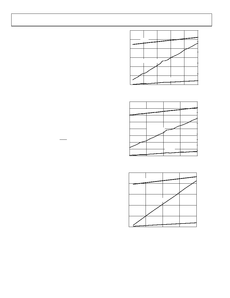
POWER DISSIPATION AND STANDBY MODE
the AD9233 is proportional to its sample rate. The digital power
dissipation is determined primarily by the strength of the digital
drivers and the load on each output bit. The maximum DRVDD
current (IDRVDD) can be calculated as
N
f
C
V
I
CLK
LOAD
DRVDD
×
=
2
where N is the number of output bits (12 in the case of the
AD9233).
This maximum current occurs when every output bit switches
on every clock cycle, that is, a full-scale square wave at the
Nyquist frequency, fCLK/2. In practice, the DRVDD current is
established by the average number of output bits switching,
which is determined by the sample rate and the characteristics
of the analog input signal. Reducing the capacitive load
presented to the output drivers can minimize digital power
consumption.
same operating conditions as used in the plots in the Typical
Performance Characteristics section with a 5 pF load on each
output driver.
475
325
0
125
CLOCK FREQUENCY (MSPS)
P
O
WE
R
(
m
W)
450
425
400
375
350
250
0
CU
RRE
NT
(
m
A)
200
150
100
50
25
50
75
100
IDRVDD
IAVDD
TOTAL POWER
05
49
2-
03
4
Figure 52. AD9233-125 Power and Current vs. Clock Frequency, FIN = 30 MHz
410
250
5
CLOCK FREQUENCY (MSPS)
PO
W
E
R
(mW
)
200
180
0
CURR
E
NT
(
m
A)
160
140
120
100
80
60
40
20
30
55
80
105
390
370
350
330
310
290
270
IDRVDD
IAVDD
TOTAL POWER
0
549
2-
0
82
Figure 53. AD9233-105 Power and Current vs. Clock Frequency, FIN = 30 MHz
290
215
0
CLOCK FREQUENCY (MSPS)
P
O
WE
R
(
m
W)
150
0
CU
RRE
NT
(
m
A)
120
90
60
30
80
IDRVDD
IAVDD
TOTAL POWER
05
49
2-
0
93
275
260
245
230
20
40
60
Figure 54. AD9233-80 Power and Current vs. Clock Frequency, FIN = 30 MHz
相关PDF资料 |
PDF描述 |
|---|---|
| IDT72221L25J8 | IC FIFO SYNC 1KX9 25NS 32PLCC |
| MS27484T16A26PA | CONN PLUG 26POS STRAIGHT W/PINS |
| MS3476W14-12P | CONN PLUG 12POS STRAIGHT W/PINS |
| IDT72215LB25PF8 | IC FIFO 512X18 SYNC 25NS 64-TQFP |
| MS27473E16F35PB | CONN PLUG 55POS STRAIGHT W/PINS |
相关代理商/技术参数 |
参数描述 |
|---|---|
| AD9233BCPZRL7-125 | 功能描述:IC ADC 12BIT 125MSPS 48-LFCSP RoHS:是 类别:集成电路 (IC) >> 数据采集 - 模数转换器 系列:- 标准包装:1 系列:- 位数:14 采样率(每秒):83k 数据接口:串行,并联 转换器数目:1 功率耗散(最大):95mW 电压电源:双 ± 工作温度:0°C ~ 70°C 安装类型:通孔 封装/外壳:28-DIP(0.600",15.24mm) 供应商设备封装:28-PDIP 包装:管件 输入数目和类型:1 个单端,双极 |
| AD9233BCPZRL7-80 | 制造商:AD 制造商全称:Analog Devices 功能描述:12-Bit, 80 MSPS/105 MSPS/125 MSPS, 1.8 V Analog-to-Digital Converter |
| AD9234-1000EBZ | 功能描述:AD9234 - 12 Bit 1G Samples per Second Analog to Digital Converter (ADC) Evaluation Board 制造商:analog devices inc. 系列:- 零件状态:有效 A/D 转换器数:2 位数:12 采样率(每秒):1G 数据接口:JESD204B 输入范围:1.34 Vpp 不同条件下的功率(典型值):3W @ 1GSPS 使用的 IC/零件:AD9234 所含物品:板 标准包装:1 |
| AD9234BCPZ-1000 | 功能描述:IC ADC 12BIT 1GSPS 64LFCSP 制造商:analog devices inc. 系列:- 包装:托盘 零件状态:在售 位数:12 采样率(每秒):1G 输入数:2 输入类型:差分 数据接口:JESD204B 配置:S/H-ADC 无线电 - S/H:ADC:1:1 A/D 转换器数:1 架构:管线 参考类型:内部 电压 - 电源,模拟:1.22 V ~ 1.28 V,2.44 V ~ 2.56 V 电压 - 电源,数字:1.22 V ~ 1.28 V 特性:- 工作温度:-40°C ~ 85°C 封装/外壳:64-WFQFN 裸露焊盘 供应商器件封装:64-LFCSP-WQ(9x9) 标准包装:1 |
| AD9234BCPZRL7-1000 | 功能描述:IC ADC 12BIT 1GSPS 64LFCSP 制造商:analog devices inc. 系列:- 包装:带卷(TR) 零件状态:在售 位数:12 采样率(每秒):1G 输入数:2 输入类型:差分 数据接口:JESD204B 配置:S/H-ADC 无线电 - S/H:ADC:1:1 A/D 转换器数:1 架构:管线 参考类型:内部 电压 - 电源,模拟:1.22 V ~ 1.28 V,2.44 V ~ 2.56 V 电压 - 电源,数字:1.22 V ~ 1.28 V 特性:- 工作温度:-40°C ~ 85°C 封装/外壳:64-VFQFN 裸露焊盘,CSP 供应商器件封装:64-LFCSP-VQ(9x9) 标准包装:750 |
发布紧急采购,3分钟左右您将得到回复。