- 您现在的位置:买卖IC网 > PDF目录10115 > AD9233BCPZRL7-105 (Analog Devices Inc)IC ADC 12BIT 105MSPS 48-LFCSP PDF资料下载
参数资料
| 型号: | AD9233BCPZRL7-105 |
| 厂商: | Analog Devices Inc |
| 文件页数: | 14/44页 |
| 文件大小: | 0K |
| 描述: | IC ADC 12BIT 105MSPS 48-LFCSP |
| 标准包装: | 750 |
| 位数: | 12 |
| 采样率(每秒): | 105M |
| 数据接口: | 串行,SPI? |
| 转换器数目: | 1 |
| 功率耗散(最大): | 350mW |
| 电压电源: | 单电源 |
| 工作温度: | -40°C ~ 85°C |
| 安装类型: | 表面贴装 |
| 封装/外壳: | 48-VFQFN 裸露焊盘,CSP |
| 供应商设备封装: | 48-LFCSP-VQ(7x7) |
| 包装: | 带卷 (TR) |
| 输入数目和类型: | 2 个单端,单极;1 个差分,单极 |
| 配用: | AD9233-125EBZ-ND - BOARD EVALUATION FOR AD9233 |
第1页第2页第3页第4页第5页第6页第7页第8页第9页第10页第11页第12页第13页当前第14页第15页第16页第17页第18页第19页第20页第21页第22页第23页第24页第25页第26页第27页第28页第29页第30页第31页第32页第33页第34页第35页第36页第37页第38页第39页第40页第41页第42页第43页第44页
AD9233
Rev. A | Page 21 of 44
Power-Down Mode
By asserting the PDWN pin high, the AD9233 is placed in
power-down mode. In this state, the ADC typically dissipates
1.8 mW. During power-down, the output drivers are placed in a
high impedance state. Reasserting the PDWN pin low returns
the AD9233 to its normal operational mode. This pin is both
1.8 V and 3.3 V tolerant.
Low power dissipation in power-down mode is achieved by
shutting down the reference, reference buffer, biasing networks,
and clock. The decoupling capacitors on REFT and REFB are
discharged when entering power-down mode and then must be
recharged when returning to normal operation. As a result, the
wake-up time is related to the time spent in power-down mode;
shorter power-down cycles result in proportionally shorter
wake-up times. With the recommended 0.1 μF decoupling
capacitor on REFT and REFB, it takes approximately 0.25 ms
to fully discharge the reference buffer decoupling capacitor and
0.35 ms to restore full operation.
Standby Mode
When using the SPI port interface, the user can place the ADC
in power-down or standby modes. Standby mode allows the
user to keep the internal reference circuitry powered when
faster wake-up times are required. See the Memory Map
section for more details.
DIGITAL OUTPUTS
The AD9233 output drivers can be configured to interface with
1.8 V to 3.3 V logic families by matching DRVDD to the digital
supply of the interfaced logic. The output drivers are sized to
provide sufficient output current to drive a wide variety of logic
families. However, large drive currents tend to cause current
glitches on the supplies that can affect converter performance.
Applications requiring the ADC to drive large capacitive loads
or large fanouts can require external buffers or latches.
The output data format can be selected for either offset binary
or twos complement by setting the SCLK/DFS pin when
operating in the external pin mode (see Table 10). As detailed in
data format can be selected for either offset binary, twos
complement, or Gray code when using the SPI control.
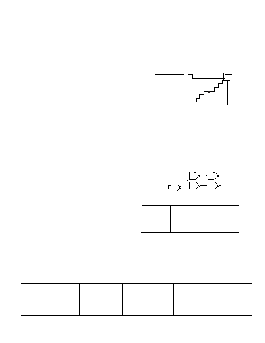
Out-of-Range (OR) Condition
An out-of-range condition exists when the analog input voltage
is beyond the input range of the ADC. OR is a digital output
that is updated along with the data output corresponding to the
particular sampled input voltage. Thus, OR has the same pipeline
latency as the digital data.
05
49
2-
0
41
1
0
1
OR DATA OUTPUTS
OR
+FS – 1 LSB
+FS – 1/2 LSB
+FS
–FS
–FS + 1/2 LSB
–FS – 1/2 LSB
1111
1110
0000
0001
0000
Figure 55. OR Relation to Input Voltage and Output Data
OR is low when the analog input voltage is within the analog
input range and high when the analog input voltage exceeds the
input range, as shown in Figure 55. OR remains high until the
analog input returns to within the input range and another
conversion is completed. By logically AND’ing the OR bit with
the MSB and its complement, overrange high or underrange
low conditions can be detected. Table 11 is a truth table for the
overrange/underrange circuit in Figure 56, which uses NAND
gates.
MSB
OR
MSB
OVER = 1
UNDER = 1
05
49
2-
0
4
5
Figure 56. Overrange/Underrange Logic
Table 11. Overrange/Underrange Truth Table
OR
MSB
Analog Input Is:
0
Within Range
0
1
Within Range
1
0
Underrange
1
Overrange
Digital Output Enable Function (OEB)
The AD9233 has three-state ability. If the OEB pin is low, the
output data drivers are enabled. If the OEB pin is high, the output
data drivers are placed in a high impedance state. This is not
intended for rapid access to the data bus. Note that OEB is
referenced to the digital supplies (DRVDD) and should not
exceed that supply voltage.
Table 12. Output Data Format
Condition (V)
Binary Output Mode
Twos Complement Mode
Gray Code Mode (SPI Accessible)
OR
VIN+ VIN < –VREF – 0.5 LSB
0000 0000 0000
1000 0000 0000
1100 0000 0000
1
VIN+ VIN = –VREF
0000 0000 0000
1000 0000 0000
1100 0000 0000
0
VIN+ VIN = 0
1000 0000 0000
0000 0000 0000
0
VIN+ VIN = +VREF – 1.0 LSB
1111 1111 1111
0111 1111 1111
1000 0000 0000
0
VIN+ VIN > +VREF – 0.5 LSB
1111 1111 1111
0111 1111 1111
1000 0000 0000
1
相关PDF资料 |
PDF描述 |
|---|---|
| IDT72221L25J8 | IC FIFO SYNC 1KX9 25NS 32PLCC |
| MS27484T16A26PA | CONN PLUG 26POS STRAIGHT W/PINS |
| MS3476W14-12P | CONN PLUG 12POS STRAIGHT W/PINS |
| IDT72215LB25PF8 | IC FIFO 512X18 SYNC 25NS 64-TQFP |
| MS27473E16F35PB | CONN PLUG 55POS STRAIGHT W/PINS |
相关代理商/技术参数 |
参数描述 |
|---|---|
| AD9233BCPZRL7-125 | 功能描述:IC ADC 12BIT 125MSPS 48-LFCSP RoHS:是 类别:集成电路 (IC) >> 数据采集 - 模数转换器 系列:- 标准包装:1 系列:- 位数:14 采样率(每秒):83k 数据接口:串行,并联 转换器数目:1 功率耗散(最大):95mW 电压电源:双 ± 工作温度:0°C ~ 70°C 安装类型:通孔 封装/外壳:28-DIP(0.600",15.24mm) 供应商设备封装:28-PDIP 包装:管件 输入数目和类型:1 个单端,双极 |
| AD9233BCPZRL7-80 | 制造商:AD 制造商全称:Analog Devices 功能描述:12-Bit, 80 MSPS/105 MSPS/125 MSPS, 1.8 V Analog-to-Digital Converter |
| AD9234-1000EBZ | 功能描述:AD9234 - 12 Bit 1G Samples per Second Analog to Digital Converter (ADC) Evaluation Board 制造商:analog devices inc. 系列:- 零件状态:有效 A/D 转换器数:2 位数:12 采样率(每秒):1G 数据接口:JESD204B 输入范围:1.34 Vpp 不同条件下的功率(典型值):3W @ 1GSPS 使用的 IC/零件:AD9234 所含物品:板 标准包装:1 |
| AD9234BCPZ-1000 | 功能描述:IC ADC 12BIT 1GSPS 64LFCSP 制造商:analog devices inc. 系列:- 包装:托盘 零件状态:在售 位数:12 采样率(每秒):1G 输入数:2 输入类型:差分 数据接口:JESD204B 配置:S/H-ADC 无线电 - S/H:ADC:1:1 A/D 转换器数:1 架构:管线 参考类型:内部 电压 - 电源,模拟:1.22 V ~ 1.28 V,2.44 V ~ 2.56 V 电压 - 电源,数字:1.22 V ~ 1.28 V 特性:- 工作温度:-40°C ~ 85°C 封装/外壳:64-WFQFN 裸露焊盘 供应商器件封装:64-LFCSP-WQ(9x9) 标准包装:1 |
| AD9234BCPZRL7-1000 | 功能描述:IC ADC 12BIT 1GSPS 64LFCSP 制造商:analog devices inc. 系列:- 包装:带卷(TR) 零件状态:在售 位数:12 采样率(每秒):1G 输入数:2 输入类型:差分 数据接口:JESD204B 配置:S/H-ADC 无线电 - S/H:ADC:1:1 A/D 转换器数:1 架构:管线 参考类型:内部 电压 - 电源,模拟:1.22 V ~ 1.28 V,2.44 V ~ 2.56 V 电压 - 电源,数字:1.22 V ~ 1.28 V 特性:- 工作温度:-40°C ~ 85°C 封装/外壳:64-VFQFN 裸露焊盘,CSP 供应商器件封装:64-LFCSP-VQ(9x9) 标准包装:750 |
发布紧急采购,3分钟左右您将得到回复。