- 您现在的位置:买卖IC网 > PDF目录10143 > AD9240ASZRL (Analog Devices Inc)IC ADC 14BIT 10MSPS 44-MQFP TR PDF资料下载
参数资料
| 型号: | AD9240ASZRL |
| 厂商: | Analog Devices Inc |
| 文件页数: | 19/24页 |
| 文件大小: | 0K |
| 描述: | IC ADC 14BIT 10MSPS 44-MQFP TR |
| 标准包装: | 800 |
| 位数: | 14 |
| 采样率(每秒): | 10M |
| 数据接口: | 并联 |
| 转换器数目: | 7 |
| 功率耗散(最大): | 330mW |
| 电压电源: | 模拟和数字 |
| 工作温度: | -40°C ~ 85°C |
| 安装类型: | 表面贴装 |
| 封装/外壳: | 44-QFP |
| 供应商设备封装: | 44-MQFP(10x10) |
| 包装: | 带卷 (TR) |
| 输入数目和类型: | 2 个单端,单极;1 个差分,单极 |
AD9240
REV.
–4–
ABSOLUTE MAXIMUM RATINGS*
With
Respect
Parameter
to
Min
Max
Units
AVDD
AVSS
–0.3
+6.5
V
DVDD
DVSS
–0.3
+6.5
V
AVSS
DVSS
–0.3
+0.3
V
AVDD
DVDD
–6.5
+6.5
V
DRVDD
DRVSS
–0.3
+6.5
V
DRVSS
AVSS
–0.3
+0.3
V
REFCOM
AVSS
–0.3
+0.3
V
CLK
AVSS
–0.3
AVDD + 0.3
V
Digital Outputs
DRVSS
–0.3
DRVDD + 0.3 V
VINA, VINB
AVSS
–0.3
AVDD + 0.3
V
VREF
AVSS
–0.3
AVDD + 0.3
V
SENSE
AVSS
–0.3
AVDD + 0.3
V
CAPB, CAPT
AVSS
–0.3
AVDD + 0.3
V
BIAS
AVSS
–0.3
AVDD + 0.3
V
Junction Temperature
+150
°C
Storage Temperature
–65
+150
°C
Lead Temperature
(10 sec)
+300
°C
*Stresses above those listed under Absolute Maximum Ratings may cause perma-
nent damage to the device. This is a stress rating only; functional operation of the
device at these or any other conditions above those indicated in the operational
sections of this specification is not implied. Exposure to absolute maximum ratings
for extended periods may effect device reliability.
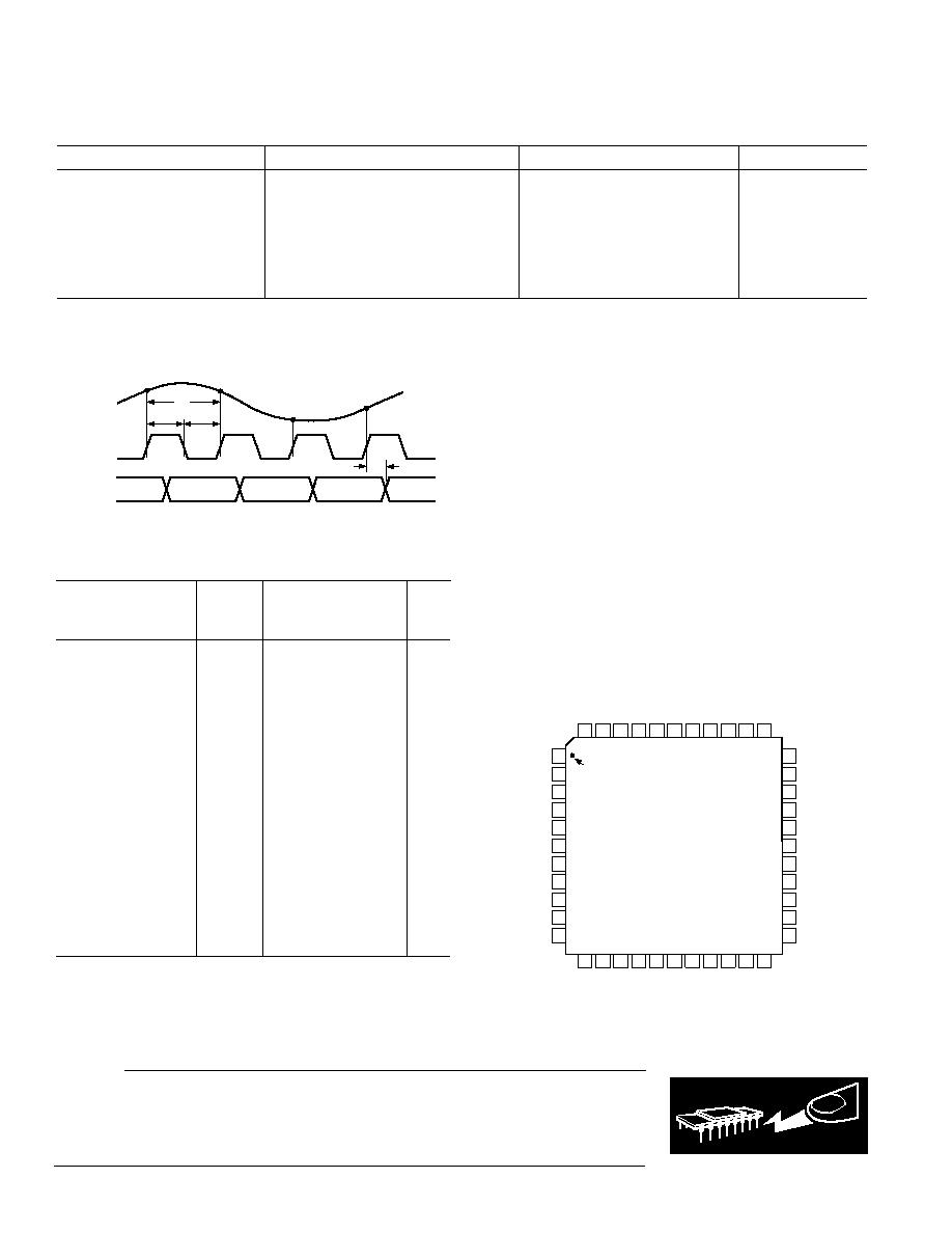
SWITCHING SPECIFICATIONS
Parameters
Symbol
AD9240
Units
Clock Period
1
tC
100
ns min
CLOCK Pulsewidth High
tCH
45
ns min
CLOCK Pulsewidth Low
tCL
45
ns min
Output Delay
tOD
8ns min
13
ns typ
19
ns max
Pipeline Delay (Latency)
3
Clock Cycles
NOTES
1The clock period may be extended to 1 ms without degradation in specified performance @ +25
°C.
Specifications subject to change without notice.
(TMIN to TMAX with AVDD = +5 V, DVDD = +5 V, DRVDD = +5 V, RBIAS = 2 k , CL = 20 pF)
CAUTION
ESD (electrostatic discharge) sensitive device. Electrostatic charges as high as 4000 V readily
accumulate on the human body and test equipment and can discharge without detection.
Although the AD9240 features proprietary ESD protection circuitry, permanent damage may
occur on devices subjected to high energy electrostatic discharges. Therefore, proper ESD
precautions are recommended to avoid performance degradation or loss of functionality.
tCL
tCH
tC
tOD
DATA 1
DATA
OUTPUT
INPUT
CLOCK
ANALOG
INPUT
S1
S2
S3
S4
Figure 1. Timing Diagram
THERMAL CHARACTERISTICS
Thermal Resistance
44-Lead MQFP
θ
JA = 53.2
°C/W
θ
JC = 19
°C/W
PIN CONFIGURATION
3
4
5
6
7
1
2
10
11
8
9
40 39 38
41
42
43
44
36 35 34
37
29
30
31
32
33
27
28
25
26
23
24
PIN 1
IDENTIFIER
TOP VIEW
(Not to Scale)
AD9240
12 13 14 15 16 17 18 19 20 21 22
NC = NO CONNECT
BIT
13
BIT
12
BIT
11
BIT
10
BIT
9
BIT
8
BIT
7
BIT
6
BIT
5
BIT
4
BIT
3
DVSS
AVSS
DVDD
AVDD
DRVSS
DRVDD
CLK
NC
(LSB) BIT 14
REFCOM
VREF
SENSE
NC
AVSS
AVDD
NC
OTR
BIT 1 (MSB)
BIT 2
NC
CML
NC
CAPT
CAPB
BIAS
NC
VINB
VINA
WARNING!
ESD SENSITIVE DEVICE
B
相关PDF资料 |
PDF描述 |
|---|---|
| IDT7201LA25SOI8 | IC MEM FIFO 512X9 25NS 28-SOIC |
| AD7880CRZ-REEL | IC ADC 12BIT MONO LP 24-SOIC |
| VI-222-IW-F4 | CONVERTER MOD DC/DC 15V 100W |
| LTC1604CG#TR | IC ADC 16BIT SAMPL SHTDWN 36SSOP |
| VE-2NX-MX-F3 | CONVERTER MOD DC/DC 5.2V 75W |
相关代理商/技术参数 |
参数描述 |
|---|---|
| AD9240EB | 制造商:AD 制造商全称:Analog Devices 功能描述:Complete 14-Bit, 10 MSPS Monolithic A/D Converter |
| AD9240-EB | 制造商:Analog Devices 功能描述: |
| AD9241 | 制造商:AD 制造商全称:Analog Devices 功能描述:Complete 14-Bit, 1.25 MSPS Monolithic A/D Converter |
| AD9241ACHIPS | 制造商:Analog Devices 功能描述: |
| AD9241AS | 制造商:Analog Devices 功能描述:ADC Single Pipelined 1.25Msps 14-bit Parallel 44-Pin MQFP 制造商:Rochester Electronics LLC 功能描述:14BIT 1.25 MSPS MONOLITHIC A/D CONVERTER - Bulk 制造商:Analog Devices 功能描述:IC 14-BIT ADC |
发布紧急采购,3分钟左右您将得到回复。