- 您现在的位置:买卖IC网 > PDF目录10143 > AD9240ASZRL (Analog Devices Inc)IC ADC 14BIT 10MSPS 44-MQFP TR PDF资料下载
参数资料
| 型号: | AD9240ASZRL |
| 厂商: | Analog Devices Inc |
| 文件页数: | 8/24页 |
| 文件大小: | 0K |
| 描述: | IC ADC 14BIT 10MSPS 44-MQFP TR |
| 标准包装: | 800 |
| 位数: | 14 |
| 采样率(每秒): | 10M |
| 数据接口: | 并联 |
| 转换器数目: | 7 |
| 功率耗散(最大): | 330mW |
| 电压电源: | 模拟和数字 |
| 工作温度: | -40°C ~ 85°C |
| 安装类型: | 表面贴装 |
| 封装/外壳: | 44-QFP |
| 供应商设备封装: | 44-MQFP(10x10) |
| 包装: | 带卷 (TR) |
| 输入数目和类型: | 2 个单端,单极;1 个差分,单极 |
AD9240
REV.
–16–
degrade slightly as the input common-mode voltage deviates
from its optimum level of 2.5 V.
Alternative AC Interface
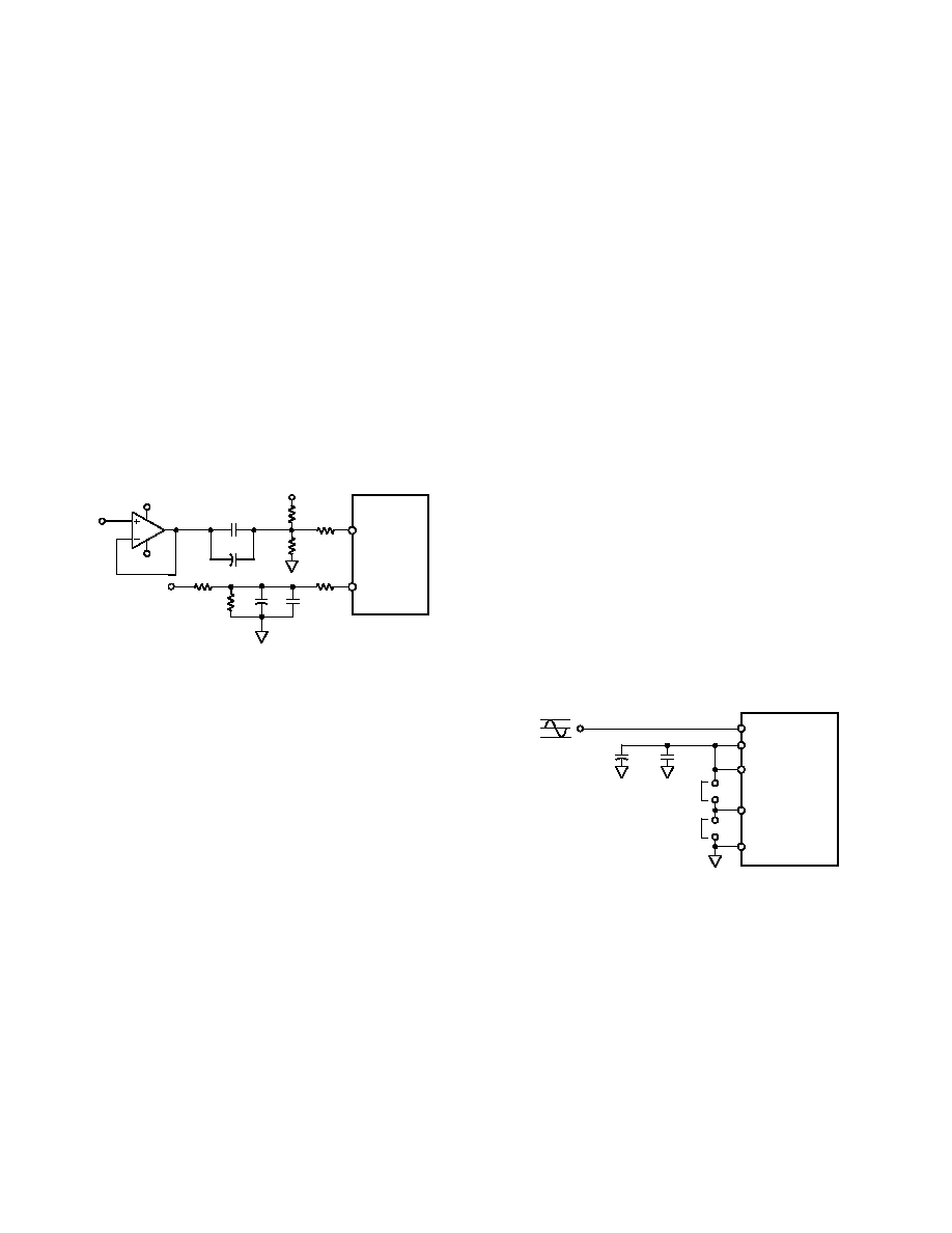
Figure 38 shows a flexible ac-coupled circuit which can be con-
figured for different input spans. Since the common-mode
voltage of VINA and VINB are biased to midsupply indepen-
dent of VREF, VREF can be pin-strapped or reconfigured to
achieve input spans between 2 V and 5 V p-p. The AD9240’s
CMRR along with the symmetrical coupling R-C networks will
reject both power supply variations and noise. The resistors, R,
establish the common-mode voltage. They may have a high value
(e.g., 5 k
) to minimize power consumption and establish a low
cutoff frequency. The capacitors, C1 and C2, are typically a
0.1
F ceramic and 10 F tantalum capacitor in parallel to
achieve a low cutoff frequency while maintaining a low imped-
ance over a wide frequency range. RS isolates the buffer ampli-
fier from the A/D input. The optimum performance is achieved
when VINA and VINB are driven via symmetrical networks.
The high pass f–3 dB point can be approximated by the equation,
f–3 dB = 1/(2 × π × R/2 × (C1 + C2))
C2
VINA
VINB
AD9240
C1
R
+5V
–5V
RS
VIN
C1
C2
R
RS
+5V
R
+5V
Figure 38. AC-Coupled Input-Flexible Input Span,
VCM = 2.5 V
OP AMP SELECTION GUIDE
Op amp selection for the AD9240 is highly dependent on a
particular application. In general, the performance requirements
of any given application can be characterized by either time
domain or frequency domain parameters. In either case, one
should carefully select an op amp that preserves the perfor-
mance of the A/D. This task becomes challenging when one
considers the AD9240’s high performance capabilities coupled
with other external system level requirements such as power
consumption and cost.
The ability to select the optimal op amp may be further compli-
cated by limited power supply availability and/or limited accept-
able supplies for a desired op amp. Newer, high performance op
amps typically have input and output range limitations in accor-
dance with their lower supply voltages. As a result, some op
amps will be more appropriate in systems where ac-coupling is
allowable. When dc-coupling is required, op amps without
headroom constraints such as rail-to-rail op amps or ones where
larger supplies can be used should be considered. The following
section describes some op amps currently available from Analog
Devices. The system designer is always encouraged to contact
the factory or local sales office to be updated on Analog De-
vices’ latest amplifier product offerings. Highlights of the areas
where the op amps excel and where they may limit the perfor-
mance of the AD9240 are also included.
AD9631:
220 MHz Unity GBW, 16 ns Settling to 0.01%,
±5 V Supplies
Best Applications: Best AC Specs, Low Noise,
AC-Coupled
Limits: Usable Input/Output Range, Power
Consumption
AD8047:
130 MHz Unity GBW, 30 ns Settling to 0.01%,
±5 V Supplies
Best Applications: Good AC Specs, Low Noise,
AC-Coupled
Limits: THD > 5 MHz, Usable Input Range
AD8042:
Dual AD8041
Best Applications: Differential and/or Low Imped-
ance Input Drivers
Limits: Noise with 2 V Input Range
REFERENCE CONFIGURATIONS
For the purpose of simplicity, the figures associated with this
section on internal and external reference operation do not
show recommended matching series resistors for VINA and
VINB. Please refer to section Driving the Analog Inputs, Intro-
duction, for a discussion of this topic. The figures do not show
the decoupling network associated with the CAPT and CAPB
pins. Please refer to the Reference Operation section for a discus-
sion of the internal reference circuitry and the recommended
decoupling network shown in Figure 30.
USING THE INTERNAL REFERENCE
Single-Ended Input with 0 to 2
VREF Range
Figure 39 shows how to connect the AD9240 for a 0 V to 2 V or
0 V to 5 V input range via pin strapping the SENSE pin. An
intermediate input range of 0 to 2
× VREF can be established
using the resistor programmable configuration in Figure 41 and
connecting VREF to VINB.
10 F
VINA
VREF
AD9240
0.1 F
VINB
2xVREF
0V
SHORT FOR 0 TO 2V
INPUT SPAN
SENSE
SHORT FOR 0 TO 5V
INPUT SPAN
REFCOM
Figure 39. Internal Reference (2 V p-p Input Span,
VCM = 1 V, or 5 V p-p Input Span, VCM = 2.5 V)
In either case, both the common-mode voltage and input span
are directly dependent on the value of VREF. More specifically,
the common-mode voltage is equal to VREF while the input
span is equal to 2
× VREF. Thus, the valid input range extends
from 0 to 2
× VREF. When VINA is ≤ 0 V, the digital output
will be 0000 Hex; when VINA is
≥ 2 × VREF, the digital output
will be 3FFF Hex.
Shorting the VREF pin directly to the SENSE pin places the
internal reference amplifier in unity-gain mode and the result-
ant VREF output is 1 V. The valid input range is, therefore, 0 V
to 2 V. Shorting the SENSE pin directly to the REFCOM pin
configures the internal reference amplifier for a gain of 2.5 and
B
相关PDF资料 |
PDF描述 |
|---|---|
| IDT7201LA25SOI8 | IC MEM FIFO 512X9 25NS 28-SOIC |
| AD7880CRZ-REEL | IC ADC 12BIT MONO LP 24-SOIC |
| VI-222-IW-F4 | CONVERTER MOD DC/DC 15V 100W |
| LTC1604CG#TR | IC ADC 16BIT SAMPL SHTDWN 36SSOP |
| VE-2NX-MX-F3 | CONVERTER MOD DC/DC 5.2V 75W |
相关代理商/技术参数 |
参数描述 |
|---|---|
| AD9240EB | 制造商:AD 制造商全称:Analog Devices 功能描述:Complete 14-Bit, 10 MSPS Monolithic A/D Converter |
| AD9240-EB | 制造商:Analog Devices 功能描述: |
| AD9241 | 制造商:AD 制造商全称:Analog Devices 功能描述:Complete 14-Bit, 1.25 MSPS Monolithic A/D Converter |
| AD9241ACHIPS | 制造商:Analog Devices 功能描述: |
| AD9241AS | 制造商:Analog Devices 功能描述:ADC Single Pipelined 1.25Msps 14-bit Parallel 44-Pin MQFP 制造商:Rochester Electronics LLC 功能描述:14BIT 1.25 MSPS MONOLITHIC A/D CONVERTER - Bulk 制造商:Analog Devices 功能描述:IC 14-BIT ADC |
发布紧急采购,3分钟左右您将得到回复。