- 您现在的位置:买卖IC网 > PDF目录10047 > AD9246BCPZRL7-125 (Analog Devices Inc)IC ADC 14BIT 125MSPS 48-LFCSP PDF资料下载
参数资料
| 型号: | AD9246BCPZRL7-125 |
| 厂商: | Analog Devices Inc |
| 文件页数: | 10/44页 |
| 文件大小: | 0K |
| 描述: | IC ADC 14BIT 125MSPS 48-LFCSP |
| 设计资源: | Using AD8376 to Drive Wide Bandwidth ADCs for High IF AC-Coupled Appls (CN0002) Driving AD9233/46/54 ADCs in AC-Coupled Baseband Appls (CN0051) |
| 标准包装: | 750 |
| 位数: | 14 |
| 采样率(每秒): | 125M |
| 数据接口: | 串行,SPI? |
| 转换器数目: | 3 |
| 功率耗散(最大): | 425mW |
| 电压电源: | 单电源 |
| 工作温度: | -40°C ~ 85°C |
| 安装类型: | 表面贴装 |
| 封装/外壳: | 48-VFQFN 裸露焊盘,CSP |
| 供应商设备封装: | 48-LFCSP-VQ(7x7) |
| 包装: | 带卷 (TR) |
| 输入数目和类型: | 2 个单端,单极;1 个差分,单极 |
第1页第2页第3页第4页第5页第6页第7页第8页第9页当前第10页第11页第12页第13页第14页第15页第16页第17页第18页第19页第20页第21页第22页第23页第24页第25页第26页第27页第28页第29页第30页第31页第32页第33页第34页第35页第36页第37页第38页第39页第40页第41页第42页第43页第44页
AD9246
Rev. A | Page 18 of 44
VREF
SENSE
0.5V
AD9246
REFT
REFB
SELECT
LOGIC
0.1F
05
49
1-
0
43
VIN–
VIN+
ADC
CORE
–
Figure 42. Internal Reference Configuration
VREF
SENSE
0.5V
AD9246
VIN–
VIN+
REFT
REFB
SELECT
LOGIC
0.1F
R2
R1
05
49
1-
04
4
0.1F
ADC
CORE
–
Figure 43. Programmable Reference Configuration
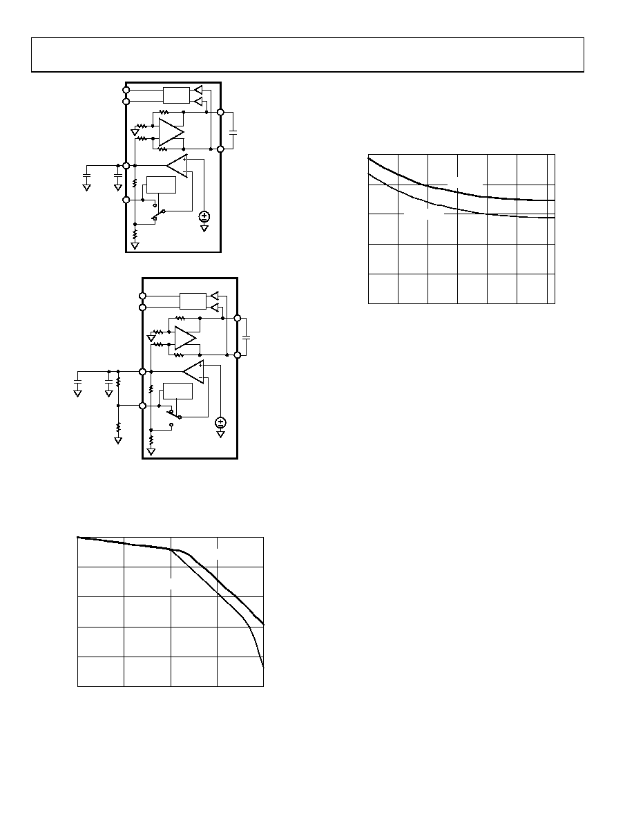
If the internal reference of the AD9246 is used to drive multiple
converters to improve gain matching, the loading of the reference
by the other converters must be considered. Figure 44 depicts
how the internal reference voltage is affected by loading.
0
–1.25
0
LOAD CURRENT (mA)
RE
F
E
RE
NCE
V
O
L
T
AG
E
RR
O
R
(
%
)
2.0
–0.25
–0.50
–0.75
–1.00
0.5
1.0
1.5
VREF = 0.5V
VREF = 1V
05
49
1-
0
33
Figure 44. VREF Accuracy vs. Load
External Reference Operation
The use of an external reference may be necessary to enhance
the gain accuracy of the ADC or improve thermal drift charac-
teristics. Figure 45 shows the typical drift characteristics of the
internal reference in both 1 V and 0.5 V modes.
–40
–20
10
0
TEMPERATURE (°C)
RE
F
E
RE
NC
E
V
O
L
T
AG
E
RRO
R
(
m
V
)
8
6
4
2
80
0
204060
VREF = 1V
VREF = 0.5V
05
49
1-
0
36
Figure 45. Typical VREF Drift
When the SENSE pin is tied to AVDD, the internal reference is
disabled, allowing the use of an external reference. An internal
resistor divider loads the external reference with an equivalent
6 kΩ load (see Figure 11). In addition, an internal buffer
generates the positive and negative full-scale references for the
ADC core. Therefore, the external reference must be limited to
a maximum of 1 V.
CLOCK INPUT CONSIDERATIONS
For optimum performance, the AD9246 sample clock inputs
(CLK+ and CLK) should be clocked with a differential signal.
The signal is typically ac-coupled into the CLK+ pin and the
CLK pin via a transformer or capacitors. These pins are biased
internally (see Figure 5) and require no external bias.
Clock Input Options
The AD9246 has a very flexible clock input structure. The clock
input can be a CMOS, LVDS, LVPECL, or sine wave signal.
Regardless of the type of signal used, the jitter of the clock
source is of the most concern (see the Jitter Considerations
section).
Figure 46 shows one preferred method for clocking the
AD9246. A low jitter clock source is converted from single-
ended to a differential signal using an RF transformer. The
back-to-back Schottky diodes across the transformer secondary
limit clock excursions into the AD9246 to approximately
0.8 V p-p differential. This helps prevent the large voltage
swings of the clock from feeding through to other portions of
the AD9246, while preserving the fast rise and fall times of the
signal, which are critical to a low jitter performance.
相关PDF资料 |
PDF描述 |
|---|---|
| MS27473T12C98S | CONN PLUG 10POS STRAIGHT W/SCKT |
| MS27497T24F61S | CONN RCPT 61POS WALL MNT W/SCKT |
| VI-2VV-MY | CONVERTER MOD DC/DC 5.8V 50W |
| VI-2VT-MY | CONVERTER MOD DC/DC 6.5V 50W |
| VI-B03-MY | CONVERTER MOD DC/DC 24V 50W |
相关代理商/技术参数 |
参数描述 |
|---|---|
| AD9246BCPZRL7-80 | 制造商:Analog Devices 功能描述:14-BIT, 80 MSPS/105 MSPS/125 MSPS, 1.8 V ANALOG-TO-DIGITAL C - Tape and Reel |
| AD9248 | 制造商:Analog Devices 功能描述:40 MSPS DUAL A/D CONVERTER - Bulk |
| AD9248-20PCB | 制造商:AD 制造商全称:Analog Devices 功能描述:14-Bit, 20/40/65 MSPS Dual A/ D Converter |
| AD9248-40PCB | 制造商:AD 制造商全称:Analog Devices 功能描述:14-Bit, 20/40/65 MSPS Dual A/ D Converter |
| AD9248-65PCB | 制造商:AD 制造商全称:Analog Devices 功能描述:14-Bit, 20/40/65 MSPS Dual A/ D Converter |
发布紧急采购,3分钟左右您将得到回复。