- 您现在的位置:买卖IC网 > PDF目录10047 > AD9246BCPZRL7-125 (Analog Devices Inc)IC ADC 14BIT 125MSPS 48-LFCSP PDF资料下载
参数资料
| 型号: | AD9246BCPZRL7-125 |
| 厂商: | Analog Devices Inc |
| 文件页数: | 11/44页 |
| 文件大小: | 0K |
| 描述: | IC ADC 14BIT 125MSPS 48-LFCSP |
| 设计资源: | Using AD8376 to Drive Wide Bandwidth ADCs for High IF AC-Coupled Appls (CN0002) Driving AD9233/46/54 ADCs in AC-Coupled Baseband Appls (CN0051) |
| 标准包装: | 750 |
| 位数: | 14 |
| 采样率(每秒): | 125M |
| 数据接口: | 串行,SPI? |
| 转换器数目: | 3 |
| 功率耗散(最大): | 425mW |
| 电压电源: | 单电源 |
| 工作温度: | -40°C ~ 85°C |
| 安装类型: | 表面贴装 |
| 封装/外壳: | 48-VFQFN 裸露焊盘,CSP |
| 供应商设备封装: | 48-LFCSP-VQ(7x7) |
| 包装: | 带卷 (TR) |
| 输入数目和类型: | 2 个单端,单极;1 个差分,单极 |
第1页第2页第3页第4页第5页第6页第7页第8页第9页第10页当前第11页第12页第13页第14页第15页第16页第17页第18页第19页第20页第21页第22页第23页第24页第25页第26页第27页第28页第29页第30页第31页第32页第33页第34页第35页第36页第37页第38页第39页第40页第41页第42页第43页第44页
AD9246
Rev. A | Page 19 of 44
0.1F
SCHOTTKY
DIODES:
HSMS2812
CLOCK
INPUT
50
100
CLK–
CLK+
ADC
AD9246
MIN-CIRCUITS
ADT1–1WT, 1:1Z
XFMR
05
49
1-
0
4
8
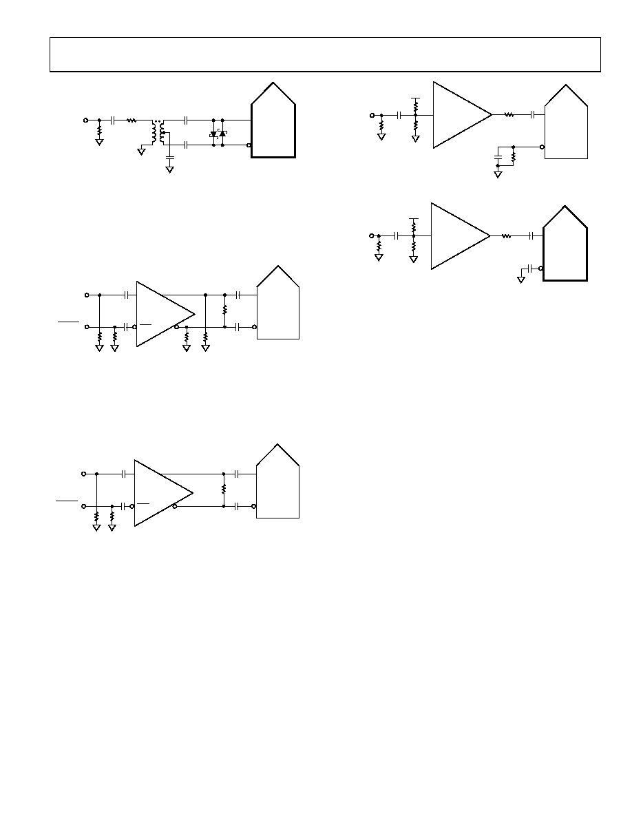
Figure 46. Transformer Coupled Differential Clock
If a low jitter clock source is not available, another option is to
ac-couple a differential PECL signal to the sample clock input
pins, as shown in Figure 47. The AD9510/AD9511/AD9512/
AD9513/AD9514/AD9515 family of clock drivers offers excel-
lent jitter performance.
100
0.1F
240
AD951x
PECL DRIVER
501
CLK
150 RESISTORS ARE OPTIONAL
CLK–
CLK+
ADC
AD9246
CLOCK
INPUT
CLOCK
INPUT
054
91
-0
49
Figure 47. Differential PECL Sample Clock
A third option is to ac-couple a differential LVDS signal to the
sample clock input pins, as shown in Figure 48. The AD9510/
AD9511/AD9512/AD9513/AD9514/AD9515 family of clock
drivers offers excellent jitter performance.
100
0.1F
501
AD951x
LVDS DRIVER
501
CLK
150 RESISTORS ARE OPTIONAL
CLK–
CLK+
CLOCK
INPUT
CLOCK
INPUT
ADC
AD9246
05491
-05
0
Figure 48. Differential LVDS Sample Clock
In some applications, it is acceptable to drive the sample clock
inputs with a single-ended CMOS signal. In such applications,
directly drive CLK+ from a CMOS gate, while bypassing the
CLK pin to ground using a 0.1 μF capacitor in parallel with a
39 kΩ resistor (see Figure 49). CLK+ may be directly driven
from a CMOS gate. This input is designed to withstand input
voltages up to 3.6 V, making the selection of the drive logic
voltage very flexible. When driving CLK+ with a 1.8 V CMOS
signal, biasing the CLK pin with a 0.1 μF capacitor in parallel
with a 39 kΩ resistor (see Figure 49) is required. The 39 kΩ
resistor is not required when driving CLK+ with a 3.3 V CMOS
signal (see Figure 50).
OPTIONAL
100
0.1F
39k
AD951x
CMOS DRIVER
501
150 RESISTOR IS OPTIONAL
CLK–
CLK+
ADC
AD9246
VCC
1k
CLOCK
INPUT
054
91-
051
Figure 49. Single-Ended 1.8 V CMOS Sample Clock
150 RESISTOR IS OPTIONAL
OPTIONAL
100
0.1F
VCC
AD951x
CMOS DRIVER
501
CLK–
CLK+
ADC
AD9246
1k
CLOCK
INPUT
05
49
1-
0
52
Figure 50. Single-Ended 3.3 V CMOS Sample Clock
Clock Duty Cycle
Typical high speed ADCs use both clock edges to generate a
variety of internal timing signals. As a result, these ADCs may
be sensitive to clock duty cycle. Commonly, a ±5% tolerance is
required on the clock duty cycle to maintain dynamic
performance characteristics.
The AD9246 contains a duty cycle stabilizer (DCS) that retimes
the nonsampling, or falling edge, providing an internal clock
signal with a nominal 50% duty cycle. This allows a wide range
of clock input duty cycles without affecting the performance of
the AD9246. Noise and distortion performance are nearly flat
for a wide range of duty cycles when the DCS is on, as shown in
Jitter in the rising edge of the input is still of paramount
concern and is not reduced by the internal stabilization circuit.
The duty cycle control loop does not function for clock rates
less than 20 MHz nominally. The loop has a time constant
associated with it that needs to be considered in applications
where the clock rate can change dynamically. This requires a
wait time of 1.5 μs to 5 μs after a dynamic clock frequency
increase (or decrease) before the DCS loop is relocked to the
input signal. During the time period the loop is not locked, the
DCS loop is bypassed, and the internal device timing is
dependent on the duty cycle of the input clock signal. In such
an application, it may be appropriate to disable the duty cycle
stabilizer. In all other applications, enabling the DCS circuit is
recommended to maximize ac performance.
相关PDF资料 |
PDF描述 |
|---|---|
| MS27473T12C98S | CONN PLUG 10POS STRAIGHT W/SCKT |
| MS27497T24F61S | CONN RCPT 61POS WALL MNT W/SCKT |
| VI-2VV-MY | CONVERTER MOD DC/DC 5.8V 50W |
| VI-2VT-MY | CONVERTER MOD DC/DC 6.5V 50W |
| VI-B03-MY | CONVERTER MOD DC/DC 24V 50W |
相关代理商/技术参数 |
参数描述 |
|---|---|
| AD9246BCPZRL7-80 | 制造商:Analog Devices 功能描述:14-BIT, 80 MSPS/105 MSPS/125 MSPS, 1.8 V ANALOG-TO-DIGITAL C - Tape and Reel |
| AD9248 | 制造商:Analog Devices 功能描述:40 MSPS DUAL A/D CONVERTER - Bulk |
| AD9248-20PCB | 制造商:AD 制造商全称:Analog Devices 功能描述:14-Bit, 20/40/65 MSPS Dual A/ D Converter |
| AD9248-40PCB | 制造商:AD 制造商全称:Analog Devices 功能描述:14-Bit, 20/40/65 MSPS Dual A/ D Converter |
| AD9248-65PCB | 制造商:AD 制造商全称:Analog Devices 功能描述:14-Bit, 20/40/65 MSPS Dual A/ D Converter |
发布紧急采购,3分钟左右您将得到回复。