- 您现在的位置:买卖IC网 > PDF目录10047 > AD9246BCPZRL7-125 (Analog Devices Inc)IC ADC 14BIT 125MSPS 48-LFCSP PDF资料下载
参数资料
| 型号: | AD9246BCPZRL7-125 |
| 厂商: | Analog Devices Inc |
| 文件页数: | 13/44页 |
| 文件大小: | 0K |
| 描述: | IC ADC 14BIT 125MSPS 48-LFCSP |
| 设计资源: | Using AD8376 to Drive Wide Bandwidth ADCs for High IF AC-Coupled Appls (CN0002) Driving AD9233/46/54 ADCs in AC-Coupled Baseband Appls (CN0051) |
| 标准包装: | 750 |
| 位数: | 14 |
| 采样率(每秒): | 125M |
| 数据接口: | 串行,SPI? |
| 转换器数目: | 3 |
| 功率耗散(最大): | 425mW |
| 电压电源: | 单电源 |
| 工作温度: | -40°C ~ 85°C |
| 安装类型: | 表面贴装 |
| 封装/外壳: | 48-VFQFN 裸露焊盘,CSP |
| 供应商设备封装: | 48-LFCSP-VQ(7x7) |
| 包装: | 带卷 (TR) |
| 输入数目和类型: | 2 个单端,单极;1 个差分,单极 |
第1页第2页第3页第4页第5页第6页第7页第8页第9页第10页第11页第12页当前第13页第14页第15页第16页第17页第18页第19页第20页第21页第22页第23页第24页第25页第26页第27页第28页第29页第30页第31页第32页第33页第34页第35页第36页第37页第38页第39页第40页第41页第42页第43页第44页
AD9246
Rev. A | Page 20 of 44
The DCS can be enabled or disabled by setting the SDIO/DCS
pin when operating in the external pin mode (see Table 10), or
via the SPI, as described in Table 13.
Table 10. Mode Selection (External Pin Mode)
Voltage at Pin
SCLK/DFS
SDIO/DCS
AGND
Binary (default)
DCS disabled
AVDD
Twos complement
DCS enabled
(default)
JITTER CONSIDERATIONS
High speed, high resolution ADCs are sensitive to the quality of
the clock input. The degradation in SNR at a given input
frequency (fIN) due to jitter (tJ) is calculated as follows:
SNR = 20 log (2π × fIN × tJ)
In the equation, the rms aperture jitter represents the root mean
square of all jitter sources, which include the clock input, analog
input signal, and ADC aperture jitter specification. IF under-
sampling applications are particularly sensitive to jitter, as
illustrated in Figure 51.
75
70
65
60
55
50
45
40
1
10
100
1000
S
NR
(
d
Bc)
INPUT FREQUENCY (MHz)
05
49
1-
0
83
3.00ps
0.05ps
MEASURED
PERFORMANCE
0.20ps
0.5ps
1.0ps
1.50ps
2.00ps
2.50ps
Figure 51. SNR vs. Input Frequency and Jitter
Treat the clock input as an analog signal in cases where aperture
jitter may affect the dynamic range of the AD9246. Power supplies
for clock drivers should be separated from the ADC output driver
supplies to avoid modulating the clock signal with digital noise.
The power supplies should also not be shared with analog input
circuits, such as buffers, to avoid the clock modulating onto the
input signal or vice versa. Low jitter, crystal-controlled oscillators
make the best clock sources. If the clock is generated from
another type of source (by gating, dividing, or other methods),
it should be retimed by the original clock at the last step.
Refer to Application Notes AN-501, Aperture Uncertainty and
ADC System Performance, and AN-756, Sampled Systems and
the Effects of Clock Phase Noise and Jitter, for more in-depth
information about jitter performance as it relates to ADCs.
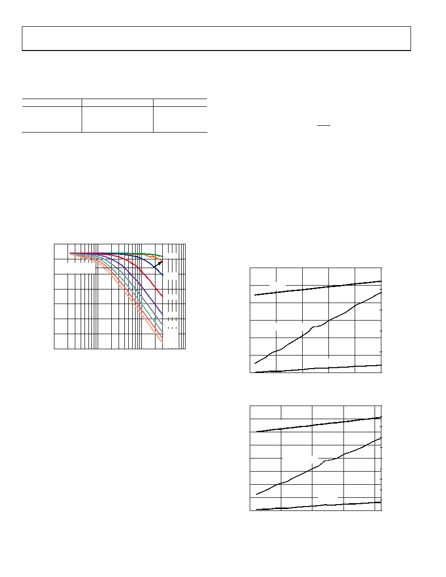
POWER DISSIPATION AND STANDBY MODE
As shown in Figure 52 and Figure 53, the power dissipated by
the AD9246 is proportional to its sample rate. The digital power
dissipation is determined primarily by the strength of the digital
drivers and the load on each output bit. The maximum DRVDD
current (IDRVDD) can be calculated as:
N
f
C
V
I
CLK
LOAD
DRVDD
×
=
2
where N is the number of output bits, 14 in the case of the
AD9246.
This maximum current occurs when every output bit switches
on every clock cycle, that is, a full-scale square wave at the
Nyquist frequency, fCLK/2. In practice, the DRVDD current is
established by the average number of output bits switching,
which is determined by the sample rate and the characteristics
of the analog input signal. Reducing the capacitive load
presented to the output drivers can minimize digital power
consumption. The data in Figure 52 and Figure 53 was taken
under the same operating conditions as the data for the Typical
Performance Characteristics section, with a 5 pF load on each
output driver.
475
325
01
CLOCK FREQUENCY (MSPS)
P
O
WE
R
(
m
W)
25
450
425
400
375
350
250
0
CU
RRE
NT
(
m
A)
200
150
100
50
25
50
75
100
IDRVDD
IAVDD
TOTAL POWER
05
49
1-
0
34
Figure 52. AD9246-125 Power and Current vs. Clock Frequency fIN = 30 MHz
410
250
0
CLOCK FREQUENCY (MSPS)
P
O
WE
R
(
m
W)
200
180
0
CU
RRE
NT
(
m
A)
160
140
120
100
80
60
40
20
25
50
75
100
390
370
350
330
310
290
270
IDRVDD
IAVDD
TOTAL POWER
05
49
1-
0
68
Figure 53. AD9246-105 Power and Current vs. Clock Frequency fIN = 30 MHz
相关PDF资料 |
PDF描述 |
|---|---|
| MS27473T12C98S | CONN PLUG 10POS STRAIGHT W/SCKT |
| MS27497T24F61S | CONN RCPT 61POS WALL MNT W/SCKT |
| VI-2VV-MY | CONVERTER MOD DC/DC 5.8V 50W |
| VI-2VT-MY | CONVERTER MOD DC/DC 6.5V 50W |
| VI-B03-MY | CONVERTER MOD DC/DC 24V 50W |
相关代理商/技术参数 |
参数描述 |
|---|---|
| AD9246BCPZRL7-80 | 制造商:Analog Devices 功能描述:14-BIT, 80 MSPS/105 MSPS/125 MSPS, 1.8 V ANALOG-TO-DIGITAL C - Tape and Reel |
| AD9248 | 制造商:Analog Devices 功能描述:40 MSPS DUAL A/D CONVERTER - Bulk |
| AD9248-20PCB | 制造商:AD 制造商全称:Analog Devices 功能描述:14-Bit, 20/40/65 MSPS Dual A/ D Converter |
| AD9248-40PCB | 制造商:AD 制造商全称:Analog Devices 功能描述:14-Bit, 20/40/65 MSPS Dual A/ D Converter |
| AD9248-65PCB | 制造商:AD 制造商全称:Analog Devices 功能描述:14-Bit, 20/40/65 MSPS Dual A/ D Converter |
发布紧急采购,3分钟左右您将得到回复。