- 您现在的位置:买卖IC网 > PDF目录16849 > AD9512/PCBZ (Analog Devices Inc)BOARD EVAL FOR AD9512 PDF资料下载
参数资料
| 型号: | AD9512/PCBZ |
| 厂商: | Analog Devices Inc |
| 文件页数: | 22/48页 |
| 文件大小: | 0K |
| 描述: | BOARD EVAL FOR AD9512 |
| 设计资源: | AD9512 Eval Brd BOM AD9511/12 All Layers AD9511/12 Schematics AD9511/12 Gerber Files |
| 标准包装: | 1 |
| 主要目的: | 计时,时钟分配 |
| 已用 IC / 零件: | AD9512 |
| 已供物品: | 板 |
第1页第2页第3页第4页第5页第6页第7页第8页第9页第10页第11页第12页第13页第14页第15页第16页第17页第18页第19页第20页第21页当前第22页第23页第24页第25页第26页第27页第28页第29页第30页第31页第32页第33页第34页第35页第36页第37页第38页第39页第40页第41页第42页第43页第44页第45页第46页第47页第48页
AD9512
Rev. A | Page 29 of 48
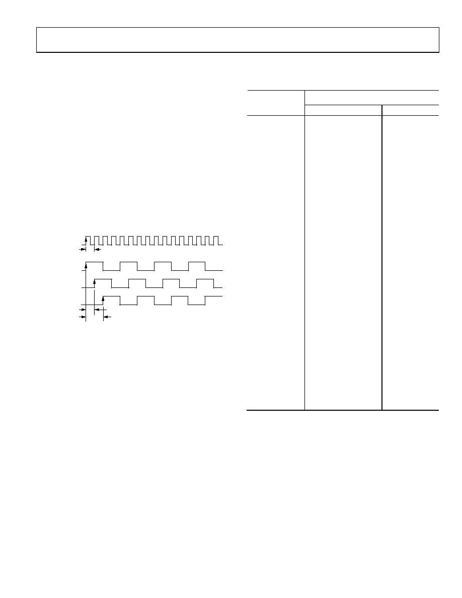
Divider Phase Offset
The phase of each output may be selected, depending on the
divide ratio chosen. This is selected by writing the appropriate
values to the registers, which set the phase and start high/low
bit for each output. These are the odd numbered registers from
4Bh to 53h. Each divider has a 4-bit phase offset <3:0> and a
start high or low bit <4>.
Following a sync pulse, the phase offset word determines how
many fast clock (CLK1 or CLK2) cycles to wait before initiating
a clock output edge. The Start H/L bit determines if the divider
output starts low or high. By giving each divider a different
phase offset, output-to-output delays can be set in increments of
the fast clock period, tCLK.
Figure 25 shows three dividers, each set for DIV = 4, 50% duty
cycle. By incrementing the phase offset from 0 to 2, each output
is offset from the initial edge by a multiple of tCLK.
05287-091
123456
789
10
11 12
13
14
15
0
CLOCK INPUT
CLK
DIVIDER OUTPUTS
DIV = 4, DUTY = 50%
START = 0,
PHASE = 0
START = 0,
PHASE = 1
START = 0,
PHASE = 2
tCLK
2
× t
CLK
Figure 25. Phase Offset—All Dividers Set for DIV = 4, Phase Set from 0 to 2
For example:
CLK1 = 491.52 MHz
tCLK1 = 1/491.52 = 2.0345 ns
For DIV = 4
Phase Offset 0 = 0 ns
Phase Offset 1 = 2.0345 ns
Phase Offset 2 = 4.069 ns
The three outputs may also be described as:
OUT1 = 0°
OUT2 = 90°
OUT3 = 180°
Setting the phase offset to Phase = 4 results in the same relative
phase as the first channel, Phase = 0° or 360°.
In general, by combining the 4-bit phase offset and the Start
H/L bit, there are 32 possible phase offset states (see Table 13).
Table 13. Phase Offset—Start H/L Bit
4Bh to 53h
Phase Offset
(Fast Clock
Rising Edges)
Phase Offset <3:0>
Start H/L <4>
0
1
0
2
0
3
0
4
0
5
0
6
0
7
0
8
0
9
0
10
0
11
0
12
0
13
0
14
0
15
0
16
0
1
17
1
18
2
1
19
3
1
20
4
1
21
5
1
22
6
1
23
7
1
24
8
1
25
9
1
26
10
1
27
11
1
28
12
1
29
13
1
30
14
1
31
15
1
The resolution of the phase offset is set by the fast clock period
(tCLK) at CLK1 or CLK2. As a result, every divide ratio does not
have 32 unique phase offsets available. For any divide ratio, the
number of unique phase offsets is numerically equal to the
divide ratio (see Table 13):
DIV = 4
Unique Phase Offsets Are Phase = 0, 1, 2, 3
DIV= 7
Unique Phase Offsets Are Phase = 0, 1, 2, 3, 4, 5, 6
相关PDF资料 |
PDF描述 |
|---|---|
| IFSC1008ABER100M01 | INDUCTOR POWER 10UH 0.75A SMD |
| AD9518-1A/PCBZ | BOARD EVALUATION FOR AD9518-1A |
| V150C5C100B | CONVERTER MOD DC/DC 5V 100W |
| AD9522-4/PCBZ | BOARD EVAL FOR AD9522-4 CLK GEN |
| AD9520-0/PCBZ | BOARD EVAL AD9520-0 |
相关代理商/技术参数 |
参数描述 |
|---|---|
| AD9512UCPZ-EP | 功能描述:IC CLOCK DIST 5OUT PLL 48LFCSP RoHS:是 类别:集成电路 (IC) >> 时钟/计时 - 时钟发生器,PLL,频率合成器 系列:- 标准包装:2,000 系列:- 类型:PLL 时钟发生器 PLL:带旁路 输入:LVCMOS,LVPECL 输出:LVCMOS 电路数:1 比率 - 输入:输出:2:11 差分 - 输入:输出:是/无 频率 - 最大:240MHz 除法器/乘法器:是/无 电源电压:3.135 V ~ 3.465 V 工作温度:0°C ~ 70°C 安装类型:表面贴装 封装/外壳:32-LQFP 供应商设备封装:32-TQFP(7x7) 包装:带卷 (TR) |
| AD9512UCPZ-EP-R7 | 功能描述:IC CLOCK DIST 5OUT PLL 48LFCSP RoHS:是 类别:集成电路 (IC) >> 时钟/计时 - 时钟发生器,PLL,频率合成器 系列:- 标准包装:2,000 系列:- 类型:PLL 时钟发生器 PLL:带旁路 输入:LVCMOS,LVPECL 输出:LVCMOS 电路数:1 比率 - 输入:输出:2:11 差分 - 输入:输出:是/无 频率 - 最大:240MHz 除法器/乘法器:是/无 电源电压:3.135 V ~ 3.465 V 工作温度:0°C ~ 70°C 安装类型:表面贴装 封装/外壳:32-LQFP 供应商设备封装:32-TQFP(7x7) 包装:带卷 (TR) |
| AD9513 | 制造商:AD 制造商全称:Analog Devices 功能描述:800 MHz Clock Distribution IC, Dividers, Delay Adjust, Three Outputs |
| AD9513/PCB | 制造商:Analog Devices 功能描述:EVAL BD FOR AD9513 ,800 MHZ CLOCK DISTRIBUTION IC, DIVIDERS, - Bulk |
| AD9513/PCBZ | 功能描述:BOARD EVAL FOR AD9513 RoHS:是 类别:编程器,开发系统 >> 评估演示板和套件 系列:- 标准包装:1 系列:PSoC® 主要目的:电源管理,热管理 嵌入式:- 已用 IC / 零件:- 主要属性:- 次要属性:- 已供物品:板,CD,电源 |
发布紧急采购,3分钟左右您将得到回复。