- 您现在的位置:买卖IC网 > PDF目录16849 > AD9512/PCBZ (Analog Devices Inc)BOARD EVAL FOR AD9512 PDF资料下载
参数资料
| 型号: | AD9512/PCBZ |
| 厂商: | Analog Devices Inc |
| 文件页数: | 40/48页 |
| 文件大小: | 0K |
| 描述: | BOARD EVAL FOR AD9512 |
| 设计资源: | AD9512 Eval Brd BOM AD9511/12 All Layers AD9511/12 Schematics AD9511/12 Gerber Files |
| 标准包装: | 1 |
| 主要目的: | 计时,时钟分配 |
| 已用 IC / 零件: | AD9512 |
| 已供物品: | 板 |
第1页第2页第3页第4页第5页第6页第7页第8页第9页第10页第11页第12页第13页第14页第15页第16页第17页第18页第19页第20页第21页第22页第23页第24页第25页第26页第27页第28页第29页第30页第31页第32页第33页第34页第35页第36页第37页第38页第39页当前第40页第41页第42页第43页第44页第45页第46页第47页第48页
AD9512
Rev. A | Page 45 of 48
Because of the limitations of single-ended CMOS clocking,
consider using differential outputs when driving high speed
signals over long traces. The AD9512 offers both LVPECL and
LVDS outputs, which are better suited for driving long traces
where the inherent noise immunity of differential signaling
provides superior performance for clocking converters.
LVDS CLOCK DISTRIBUTION
Low voltage differential signaling (LVDS) is a second
differential output option for the AD9512. LVDS uses a current
mode output stage with several user-selectable current levels.
The normal value (default) for this current is 3.5 mA, which
yields 350 mV output swing across a 100 Ω resistor. The LVDS
outputs meet or exceed all ANSI/TIA/EIA—644 specifications.
LVPECL CLOCK DISTRIBUTION
The low voltage, positive emitter-coupled, logic (LVPECL)
outputs of the AD9512 provide the lowest jitter clock signals
available from the AD9512. The LVPECL outputs (because they
are open emitter) require a dc termination to bias the output
transistors. A simplified equivalent circuit in Figure 27 shows
the LVPECL output stage.
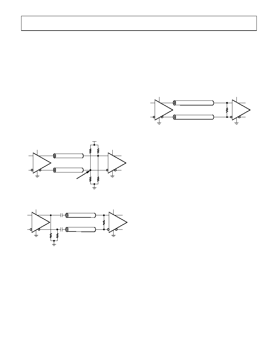
A recommended termination circuit for the LVDS outputs is
shown in Figure 44.
05287-
032
3.3V
LVDS
100
Ω
DIFFERENTIAL (COUPLED)
3.3V
LVDS
100
Ω
In most applications, a standard LVPECL far-end termination is
recommended, as shown in Figure 42. The resistor network is
designed to match the transmission line impedance (50 Ω) and
the desired switching threshold (1.3 V).
Figure 44. LVDS Output Termination
05287-
030
3.3V
LVPECL
50
Ω
50
Ω
SINGLE-ENDED
(NOT COUPLED)
3.3V
LVPECL
127
Ω
127
Ω
83
Ω
83
Ω
VT = VCC – 1.3V
See Application Note AN-586 on the ADI website at
www.analog.com for more information on LVDS.
POWER AND GROUNDING CONSIDERATIONS AND
POWER SUPPLY REJECTION
Many applications seek high speed and performance under less
than ideal operating conditions. In these application circuits,
the implementation and construction of the PCB is as
important as the circuit design. Proper RF techniques must be
used for device selection, placement, and routing, as well as for
power supply bypassing and grounding to ensure optimum
performance.
Figure 42. LVPECL Far-End Termination
05287-
031
3.3V
LVPECL
DIFFERENTIAL
(COUPLED)
3.3V
LVPECL
100
Ω
0.1nF
200
Ω
200
Ω
Figure 43. LVPECL with Parallel Transmission Line
相关PDF资料 |
PDF描述 |
|---|---|
| IFSC1008ABER100M01 | INDUCTOR POWER 10UH 0.75A SMD |
| AD9518-1A/PCBZ | BOARD EVALUATION FOR AD9518-1A |
| V150C5C100B | CONVERTER MOD DC/DC 5V 100W |
| AD9522-4/PCBZ | BOARD EVAL FOR AD9522-4 CLK GEN |
| AD9520-0/PCBZ | BOARD EVAL AD9520-0 |
相关代理商/技术参数 |
参数描述 |
|---|---|
| AD9512UCPZ-EP | 功能描述:IC CLOCK DIST 5OUT PLL 48LFCSP RoHS:是 类别:集成电路 (IC) >> 时钟/计时 - 时钟发生器,PLL,频率合成器 系列:- 标准包装:2,000 系列:- 类型:PLL 时钟发生器 PLL:带旁路 输入:LVCMOS,LVPECL 输出:LVCMOS 电路数:1 比率 - 输入:输出:2:11 差分 - 输入:输出:是/无 频率 - 最大:240MHz 除法器/乘法器:是/无 电源电压:3.135 V ~ 3.465 V 工作温度:0°C ~ 70°C 安装类型:表面贴装 封装/外壳:32-LQFP 供应商设备封装:32-TQFP(7x7) 包装:带卷 (TR) |
| AD9512UCPZ-EP-R7 | 功能描述:IC CLOCK DIST 5OUT PLL 48LFCSP RoHS:是 类别:集成电路 (IC) >> 时钟/计时 - 时钟发生器,PLL,频率合成器 系列:- 标准包装:2,000 系列:- 类型:PLL 时钟发生器 PLL:带旁路 输入:LVCMOS,LVPECL 输出:LVCMOS 电路数:1 比率 - 输入:输出:2:11 差分 - 输入:输出:是/无 频率 - 最大:240MHz 除法器/乘法器:是/无 电源电压:3.135 V ~ 3.465 V 工作温度:0°C ~ 70°C 安装类型:表面贴装 封装/外壳:32-LQFP 供应商设备封装:32-TQFP(7x7) 包装:带卷 (TR) |
| AD9513 | 制造商:AD 制造商全称:Analog Devices 功能描述:800 MHz Clock Distribution IC, Dividers, Delay Adjust, Three Outputs |
| AD9513/PCB | 制造商:Analog Devices 功能描述:EVAL BD FOR AD9513 ,800 MHZ CLOCK DISTRIBUTION IC, DIVIDERS, - Bulk |
| AD9513/PCBZ | 功能描述:BOARD EVAL FOR AD9513 RoHS:是 类别:编程器,开发系统 >> 评估演示板和套件 系列:- 标准包装:1 系列:PSoC® 主要目的:电源管理,热管理 嵌入式:- 已用 IC / 零件:- 主要属性:- 次要属性:- 已供物品:板,CD,电源 |
发布紧急采购,3分钟左右您将得到回复。