参数资料
| 型号: | AD9513BCPZ |
| 厂商: | Analog Devices Inc |
| 文件页数: | 16/28页 |
| 文件大小: | 0K |
| 描述: | IC CLOCK DIST 3OUT PLL 32LFCSP |
| 标准包装: | 1 |
| 类型: | 扇出缓冲器(分配),除法器 |
| PLL: | 无 |
| 输入: | 时钟 |
| 输出: | CMOS,LVDS |
| 电路数: | 1 |
| 比率 - 输入:输出: | 1:3 |
| 差分 - 输入:输出: | 是/是 |
| 频率 - 最大: | 800MHz |
| 除法器/乘法器: | 是/无 |
| 电源电压: | 3.135 V ~ 3.465 V |
| 工作温度: | -40°C ~ 85°C |
| 安装类型: | 表面贴装 |
| 封装/外壳: | 32-VFQFN 裸露焊盘,CSP |
| 供应商设备封装: | 32-LFCSP-VQ(5x5) |
| 包装: | 托盘 |
| 产品目录页面: | 776 (CN2011-ZH PDF) |
| 配用: | AD9513/PCBZ-ND - BOARD EVAL FOR AD9513 |
第1页第2页第3页第4页第5页第6页第7页第8页第9页第10页第11页第12页第13页第14页第15页当前第16页第17页第18页第19页第20页第21页第22页第23页第24页第25页第26页第27页第28页
AD9513
Rev. 0 | Page 23 of 28
APPLICATIONS
USING THE AD9513 OUTPUTS FOR ADC CLOCK
APPLICATIONS
Any high speed, analog-to-digital converter (ADC) is extremely
sensitive to the quality of the sampling clock provided by the
user. An ADC can be thought of as a sampling mixer; any noise,
distortion, or timing jitter on the clock is combined with the
desired signal at the A/D output. Clock integrity requirements
scale with the analog input frequency and resolution, with
higher analog input frequency applications at ≥14-bit resolution
being the most stringent. The theoretical SNR of an ADC is
limited by the ADC resolution and the jitter on the sampling
clock. Considering an ideal ADC of infinite resolution where
the step size and quantization error can be ignored, the available
SNR can be expressed approximately by
×
=
j
ft
SNR
2π
1
log
20
where f is the highest analog frequency being digitized.
tj is the rms jitter on the sampling clock.
Figure 29 shows the required sampling clock jitter as a function
of the analog frequency and effective number of bits (ENOB).
fA FULL-SCALE SINE WAVE ANALOG FREQUENCY (MHz)
SN
R
(d
B
)
EN
O
B
10
1k
100
30
40
50
60
70
80
90
100
110
6
8
10
12
14
16
18
T
J
= 100f
S
200f
S
400f
S
1ps
2ps
10ps
SNR = 20log
1
2
πfATJ
05
595
-0
91
Figure 29. ENOB and SNR vs. Analog Input Frequency
See Application Note AN-756 and Application Note AN-501 at
Many high performance ADCs feature differential clock inputs
to simplify the task of providing the required low jitter clock on
a noisy PCB. (Distributing a single-ended clock on a noisy PCB
can result in coupled noise on the sample clock. Differential
distribution has inherent common-mode rejection that can
provide superior clock performance in a noisy environment.)
The AD9513 features LVDS outputs that provide differential
clock outputs, which enable clock solutions that maximize
converter SNR performance. The input requirements of the
ADC (differential or single-ended, logic level, termination)
should be considered when selecting the best clocking/
converter solution.
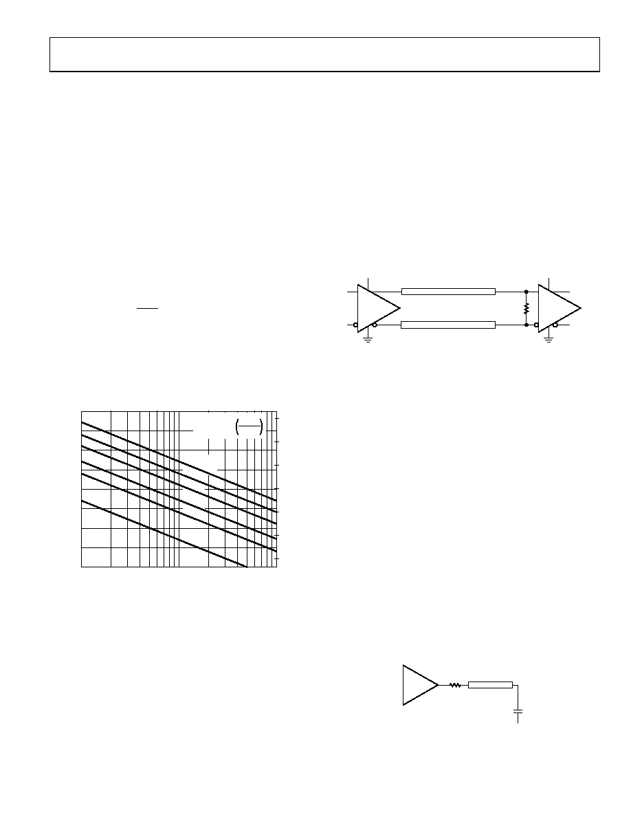
LVDS CLOCK DISTRIBUTION
The AD9513 provides three clock outputs that are selectable as
either CMOS or LVDS levels. LVDS uses a current mode output
stage. The current is 3.5 mA, which yields 350 mV output swing
across a 100 Ω resistor. The LVDS outputs meet or exceed all
ANSI/TIA/EIA-644 specifications.
A recommended termination circuit for the LVDS outputs
is shown in Figure 30.
VS
LVDS
100
DIFFERENTIAL (COUPLED)
VS
LVDS
100
05
595-
032
Figure 30. LVDS Output Termination
See Application Note AN-586 at www.analog.com for more
information on LVDS.
CMOS CLOCK DISTRIBUTION
The AD9513 provides three outputs that are selectable as either
CMOS or LVDS levels. When selected as CMOS, an output
provides for driving devices requiring CMOS level logic at their
clock inputs.
Whenever single-ended CMOS clocking is used, some of the
following general guidelines should be used.
Point-to-point nets should be designed such that a driver has
one receiver only on the net, if possible. This allows for simple
termination schemes and minimizes ringing due to possible
mismatched impedances on the net. Series termination at the
source is generally required to provide transmission line
matching and/or to reduce current transients at the driver.
The value of the resistor is dependent on the board design and
timing requirements (typically 10 Ω to 100 Ω is used). CMOS
outputs are also limited in terms of the capacitive load or trace
length that they can drive. Typically, trace lengths less than
3 inches are recommended to preserve signal rise/fall times
and preserve signal integrity.
10
MICROSTRIP
GND
5pF
60.4
1.0 INCH
CMOS
0
55
95-
0
33
Figure 31. Series Termination of CMOS Output
相关PDF资料 |
PDF描述 |
|---|---|
| SY10E167JZ | IC MUX/REGISTER 6BIT 2:1 28PLCC |
| AD9572ACPZLVD | IC PLL CLOCK GEN 25MHZ 40LFCSP |
| SY89546UMG | IC MUX 4:1 LVDS DIFF 2.5V 32MLF |
| AD9552BCPZ | IC PLL CLOCK GEN LP 32LFCSP |
| VE-JVR-MZ-S | CONVERTER MOD DC/DC 7.5V 25W |
相关代理商/技术参数 |
参数描述 |
|---|---|
| AD9513BCPZ-REEL7 | 功能描述:IC CLOCK DIST 3OUT PLL 32LFCSP RoHS:是 类别:集成电路 (IC) >> 时钟/计时 - 时钟发生器,PLL,频率合成器 系列:- 标准包装:1,000 系列:Precision Edge® 类型:时钟/频率合成器 PLL:无 输入:CML,PECL 输出:CML 电路数:1 比率 - 输入:输出:2:1 差分 - 输入:输出:是/是 频率 - 最大:10.7GHz 除法器/乘法器:无/无 电源电压:2.375 V ~ 3.6 V 工作温度:-40°C ~ 85°C 安装类型:表面贴装 封装/外壳:16-VFQFN 裸露焊盘,16-MLF? 供应商设备封装:16-MLF?(3x3) 包装:带卷 (TR) 其它名称:SY58052UMGTRSY58052UMGTR-ND |
| AD9514 | 制造商:AD 制造商全称:Analog Devices 功能描述:1.6 GHz Clock Distribution IC, Dividers, Delay Adjust, Three Outputs |
| AD9514/PCB | 制造商:Analog Devices 功能描述:CLOCK DISTRIBUTION - Bulk |
| AD9514/PCBZ | 功能描述:BOARD EVAL CLOCK 3CH AD9514 RoHS:是 类别:编程器,开发系统 >> 评估演示板和套件 系列:- 标准包装:1 系列:- 主要目的:电信,线路接口单元(LIU) 嵌入式:- 已用 IC / 零件:IDT82V2081 主要属性:T1/J1/E1 LIU 次要属性:- 已供物品:板,电源,线缆,CD 其它名称:82EBV2081 |
| AD9514BCPZ | 功能描述:IC CLOCK DIST 3OUT PLL 32LFCSP RoHS:是 类别:集成电路 (IC) >> 时钟/计时 - 时钟发生器,PLL,频率合成器 系列:- 标准包装:2,000 系列:- 类型:PLL 频率合成器 PLL:是 输入:晶体 输出:时钟 电路数:1 比率 - 输入:输出:1:1 差分 - 输入:输出:无/无 频率 - 最大:1GHz 除法器/乘法器:是/无 电源电压:4.5 V ~ 5.5 V 工作温度:-20°C ~ 85°C 安装类型:表面贴装 封装/外壳:16-LSSOP(0.175",4.40mm 宽) 供应商设备封装:16-SSOP 包装:带卷 (TR) 其它名称:NJW1504V-TE1-NDNJW1504V-TE1TR |
发布紧急采购,3分钟左右您将得到回复。