参数资料
| 型号: | AD9513BCPZ |
| 厂商: | Analog Devices Inc |
| 文件页数: | 9/28页 |
| 文件大小: | 0K |
| 描述: | IC CLOCK DIST 3OUT PLL 32LFCSP |
| 标准包装: | 1 |
| 类型: | 扇出缓冲器(分配),除法器 |
| PLL: | 无 |
| 输入: | 时钟 |
| 输出: | CMOS,LVDS |
| 电路数: | 1 |
| 比率 - 输入:输出: | 1:3 |
| 差分 - 输入:输出: | 是/是 |
| 频率 - 最大: | 800MHz |
| 除法器/乘法器: | 是/无 |
| 电源电压: | 3.135 V ~ 3.465 V |
| 工作温度: | -40°C ~ 85°C |
| 安装类型: | 表面贴装 |
| 封装/外壳: | 32-VFQFN 裸露焊盘,CSP |
| 供应商设备封装: | 32-LFCSP-VQ(5x5) |
| 包装: | 托盘 |
| 产品目录页面: | 776 (CN2011-ZH PDF) |
| 配用: | AD9513/PCBZ-ND - BOARD EVAL FOR AD9513 |
第1页第2页第3页第4页第5页第6页第7页第8页当前第9页第10页第11页第12页第13页第14页第15页第16页第17页第18页第19页第20页第21页第22页第23页第24页第25页第26页第27页第28页
AD9513
Rev. 0 | Page 17 of 28
FUNCTIONAL DESCRIPTION
OVERALL
The AD9513 provides for the distribution of its input clock on
up to three outputs. Each output can be set to either LVDS or
CMOS logic levels. Each output has its own divider that can be
set for a divide ratio selected from a list of integer values from
1 (bypassed) to 32.
OUT2 includes an analog delay block that can be set to add an
additional delay of 1.8 ns, 6.0 ns, or 11.6 ns full scale, each with
16 levels of fine adjustment.
CLK, CLKB—DIFFERENTIAL CLOCK INPUT
The CLK and CLKB pins are differential clock input pins.
This input works up to 1600 MHz. The jitter performance is
degraded by a slew rate below 1 V/ns. The input level should be
between approximately 150 mV p-p to no more than 2 V p-p.
Anything greater can result in turning on the protection diodes
on the input pins.
See Figure 18 for the CLK equivalent input circuit. This input
is fully differential and self-biased. The signal should be ac-
coupled using capacitors. If a single-ended input must be used,
this can be accommodated by ac coupling to one side of the
differential input only. The other side of the input should be
bypassed to a quiet ac ground by a capacitor.
2.5k
5k
2.5k
CLKB
CLK
VS
CLOCK INPUT
STAGE
055
95-
021
Figure 18. Clock Input Equivalent Circuit
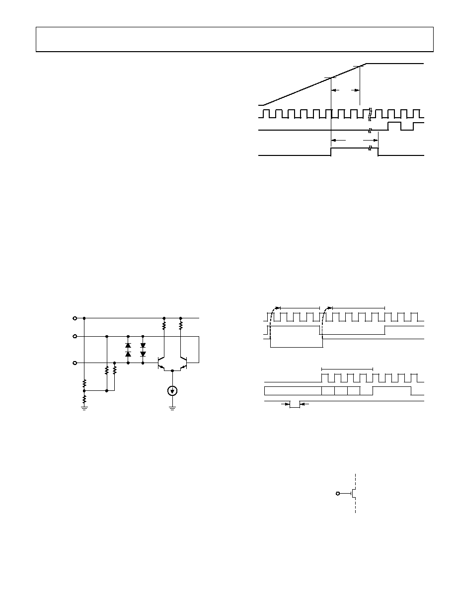
SYNCHRONIZATION
Power-On SYNC
A power-on sync (POS) is issued when the VS power supply is
turned on to ensure that the outputs start in synchronization.
The power-on sync works only if the VS power supply transi-
tions the region from 2.2 V to 3.1 V within 35 ms. The POS can
occur up to 65 ms after VS crosses 2.2 V. Only outputs which are
not divide = 1 are synchronized.
CLK
OUT
0V
3.3V
2.2V
3.1V
VS
CLOCK FREQUENCY
IS EXAMPLE ONLY
DIVIDE = 2
PHASE = 0
< 65ms
INTERNAL SYNC NODE
35ms
MAX
0559
5-
094
Figure 19. Power-On Sync Timing
SYNCB
If the setup configuration of the AD9513 is changed during
operation, the outputs can become unsynchronized. The
outputs can be resynchronized to each other at any time.
Synchronization occurs when the SYNCB pin is pulled low and
released. The clock outputs (except where divide = 1) are forced
into a fixed state (determined by the divide and phase settings)
and held there in a static condition, until the SYNCB pin is
returned to high. Upon release of the SYNCB pin, after four
cycles of the clock signal at CLK, all outputs continue clocking
in synchronicity (except where divide = 1).
When divide = 1 for an output, that output is not affected by
SYNCB.
CLK
SYNCB
OUT
3 CLK CYCLES
4 CLK CYCLES
EXAMPLE: DIVIDE ≥ 8
PHASE = 0
EXAMPLE DIVIDE
RATIO PHASE = 0
05
595
-0
93
Figure 20. SYNCB Timing with Clock Present
4 CLK CYCLES
CLK
OUT
SYNCB
DEPENDS ON PREVIOUS STATE AND DIVIDE RATIO
§§
§
DEPENDS ON PREVIOUS STATE
EXAMPLE DIVIDE
RATIO PHASE = 0
MIN 5ns
05595-
092
Figure 21. SYNCB Timing with No Clock Present
The outputs of the AD9513 can be synchronized by using the
SYNCB pin. Synchronization aligns the phases of the clock
outputs, respecting any phase offset that has been set on an
output’s divider.
SYNCB
05595
-022
Figure 22. SYNCB Equivalent Input Circuit
相关PDF资料 |
PDF描述 |
|---|---|
| SY10E167JZ | IC MUX/REGISTER 6BIT 2:1 28PLCC |
| AD9572ACPZLVD | IC PLL CLOCK GEN 25MHZ 40LFCSP |
| SY89546UMG | IC MUX 4:1 LVDS DIFF 2.5V 32MLF |
| AD9552BCPZ | IC PLL CLOCK GEN LP 32LFCSP |
| VE-JVR-MZ-S | CONVERTER MOD DC/DC 7.5V 25W |
相关代理商/技术参数 |
参数描述 |
|---|---|
| AD9513BCPZ-REEL7 | 功能描述:IC CLOCK DIST 3OUT PLL 32LFCSP RoHS:是 类别:集成电路 (IC) >> 时钟/计时 - 时钟发生器,PLL,频率合成器 系列:- 标准包装:1,000 系列:Precision Edge® 类型:时钟/频率合成器 PLL:无 输入:CML,PECL 输出:CML 电路数:1 比率 - 输入:输出:2:1 差分 - 输入:输出:是/是 频率 - 最大:10.7GHz 除法器/乘法器:无/无 电源电压:2.375 V ~ 3.6 V 工作温度:-40°C ~ 85°C 安装类型:表面贴装 封装/外壳:16-VFQFN 裸露焊盘,16-MLF? 供应商设备封装:16-MLF?(3x3) 包装:带卷 (TR) 其它名称:SY58052UMGTRSY58052UMGTR-ND |
| AD9514 | 制造商:AD 制造商全称:Analog Devices 功能描述:1.6 GHz Clock Distribution IC, Dividers, Delay Adjust, Three Outputs |
| AD9514/PCB | 制造商:Analog Devices 功能描述:CLOCK DISTRIBUTION - Bulk |
| AD9514/PCBZ | 功能描述:BOARD EVAL CLOCK 3CH AD9514 RoHS:是 类别:编程器,开发系统 >> 评估演示板和套件 系列:- 标准包装:1 系列:- 主要目的:电信,线路接口单元(LIU) 嵌入式:- 已用 IC / 零件:IDT82V2081 主要属性:T1/J1/E1 LIU 次要属性:- 已供物品:板,电源,线缆,CD 其它名称:82EBV2081 |
| AD9514BCPZ | 功能描述:IC CLOCK DIST 3OUT PLL 32LFCSP RoHS:是 类别:集成电路 (IC) >> 时钟/计时 - 时钟发生器,PLL,频率合成器 系列:- 标准包装:2,000 系列:- 类型:PLL 频率合成器 PLL:是 输入:晶体 输出:时钟 电路数:1 比率 - 输入:输出:1:1 差分 - 输入:输出:无/无 频率 - 最大:1GHz 除法器/乘法器:是/无 电源电压:4.5 V ~ 5.5 V 工作温度:-20°C ~ 85°C 安装类型:表面贴装 封装/外壳:16-LSSOP(0.175",4.40mm 宽) 供应商设备封装:16-SSOP 包装:带卷 (TR) 其它名称:NJW1504V-TE1-NDNJW1504V-TE1TR |
发布紧急采购,3分钟左右您将得到回复。