参数资料
| 型号: | AD9518-3ABCPZ |
| 厂商: | Analog Devices Inc |
| 文件页数: | 24/64页 |
| 文件大小: | 0K |
| 描述: | IC CLOCK GEN 6CH 2GHZ 48LFCSP |
| 标准包装: | 1 |
| 类型: | 时钟发生器,扇出配送 |
| PLL: | 是 |
| 输入: | CMOS,LVDS,LVPECL |
| 输出: | LVPECL |
| 电路数: | 1 |
| 比率 - 输入:输出: | 1:6 |
| 差分 - 输入:输出: | 是/是 |
| 频率 - 最大: | 2.25GHz |
| 除法器/乘法器: | 是/无 |
| 电源电压: | 3.135 V ~ 3.465 V |
| 工作温度: | -40°C ~ 85°C |
| 安装类型: | 表面贴装 |
| 封装/外壳: | 48-VFQFN 裸露焊盘,CSP |
| 供应商设备封装: | 48-LFCSP-VQ(7x7) |
| 包装: | 托盘 |
第1页第2页第3页第4页第5页第6页第7页第8页第9页第10页第11页第12页第13页第14页第15页第16页第17页第18页第19页第20页第21页第22页第23页当前第24页第25页第26页第27页第28页第29页第30页第31页第32页第33页第34页第35页第36页第37页第38页第39页第40页第41页第42页第43页第44页第45页第46页第47页第48页第49页第50页第51页第52页第53页第54页第55页第56页第57页第58页第59页第60页第61页第62页第63页第64页
AD9518-3
Data Sheet
Rev. B | Page 30 of 64
DIGITAL LOCK DETECT (DLD)
By selecting the proper output through the mux on each pin,
the DLD function can be made available at the LD, STATUS,
and REFMON pins. The DLD circuit indicates a lock when the
time difference of the rising edges at the PFD inputs is less than
a specified value (the lock threshold). The loss of a lock is
indicated when the time difference exceeds a specified value
(the unlock threshold). Note that the unlock threshold is wider
than the lock threshold, which allows some phase error in
excess of the lock window to occur without chattering on the
lock indicator.
The lock detect window timing depends on three settings:
the digital lock detect window bit (Register 0x018[4]), the
antibacklash pulse width setting (Register 0x017[1:0], see Table 2),
and the lock detect counter (Register 0x018[6:5]). A lock is not
indicated until there is a programmable number of consecutive
PFD cycles with a time difference that is less than the lock detect
threshold. The lock detect circuit continues to indicate a lock
until a time difference greater than the unlock threshold occurs
on a single subsequent cycle. For the lock detect to work properly,
the period of the PFD frequency must be greater than the unlock
threshold. The number of consecutive PFD cycles required for
lock is programmable (Register 0x018[6:5]).
Analog Lock Detect (ALD)
The AD9518 provides an ALD function that can be selected for
use at the LD pin. There are two versions of ALD, as follows:
N-channel open-drain lock detect. This signal requires a
pull-up resistor to the positive supply, VS. The output is
normally high with short, low-going pulses. Lock is indicated
by the minimum duty cycle of the low-going pulses.
P-channel open-drain lock detect. This signal requires a
pull-down resistor to GND. The output is normally low
with short, high-going pulses. Lock is indicated by the
minimum duty cycle of the high-going pulses.
The analog lock detect function requires an R-C filter to
provide a logic level indicating lock/unlock.
AD9518-3
ALD
LD
R1
C
VOUT
R2
VS = 3.3V
0
64
32
-0
67
Figure 35. Example of Analog Lock Detect Filter
Using an N-Channel Open-Drain Driver
Current Source Digital Lock Detect (DLD)
During the PLL locking sequence, it is normal for the DLD
signal to toggle a number of times before remaining steady
when the PLL is completely locked and stable. There may be
applications where it is desirable to have DLD asserted only
after the PLL is solidly locked. This is made possible by using
the current source lock detect function.
This function is set when it is selected as the output from the
LD pin control (Register 0x01A[5:0]). The current source lock
detect provides a current of 110 μA when DLD is true, and it
shorts to ground when DLD is false. If a capacitor is connected
to the LD pin, it charges at a rate that is determined by the current
source during the DLD true time but is discharged nearly instantly
when DLD is false. By monitoring the voltage at the LD pin (top
of the capacitor), it is possible to get a logic high level only after
the DLD has been true for a sufficiently long time. Any momentary
DLD false resets the charging. By selecting a properly sized
capacitor, it is possible to delay a lock detect indication until
the PLL is stably locked and the lock detect does not chatter.
The voltage on the capacitor can be sensed by an external
comparator connected to the LD pin. However, there is an
internal LD pin comparator that can be read at the REFMON
pin control (Register 0x01B[4:0]) or the STATUS pin control
(Register 0x017[7:2]) as an active high signal. It is also available
as an active low signal (REFMON, Register 0x01B[4:0] and
STATUS, Register 0x017[7:2]). The internal LD pin comparator
trip point and hysteresis are listed in Table 15.
AD9518-3
LD
REFMON
OR
STATUS
C
VOUT
110A
DLD
LD PIN
COMPARATOR
06
43
2-
0
68
Figure 36. Current Source Digital Lock Detect
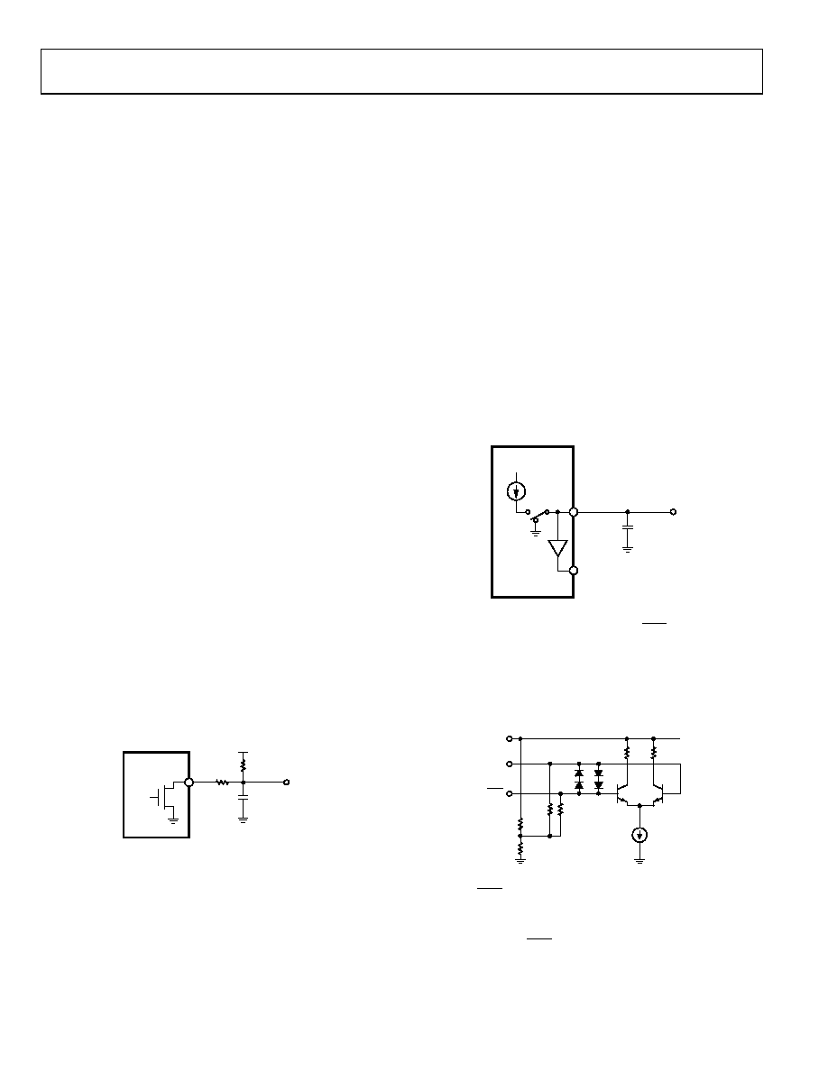
External VCXO/VCO Clock Input (CLK/CLK)
CLK is a differential input that can be used as an input to drive
the AD9518 clock distribution section. This input can receive
up to 2.4 GHz. The pins are internally self-biased, and the input
signal should be ac-coupled via capacitors.
VS
CLOCK INPUT
STAGE
CLK
5k
2.5k
0
643
2-
0
32
Figure 37. CLK Equivalent Input Circuit
The CLK/CLK input can be used either as a distribution-only
input (with the PLL off), or as a feedback input for an external
VCO/VCXO using the internal PLL when the internal VCO is
not used. The CLK/CLK input can be used for frequencies up
to 2.4 GHz.
相关PDF资料 |
PDF描述 |
|---|---|
| AD9518-4ABCPZ-RL7 | IC CLOCK GEN 6CH 1.8GHZ 48LFCSP |
| AD9520-0BCPZ-REEL7 | IC CLOCK GEN 2.8GHZ VCO 64LFCSP |
| AD9520-1BCPZ | IC CLOCK GEN 2.5GHZ VCO 64LFCSP |
| AD9520-2BCPZ | IC CLOCK GEN 2.2GHZ VCO 64LFCSP |
| AD9520-3BCPZ-REEL7 | IC CLOCK GEN 2GHZ VCO 64LFCSP |
相关代理商/技术参数 |
参数描述 |
|---|---|
| AD9518-3ABCPZ-RL7 | 功能描述:IC CLOCK GEN 6CH 2GHZ 48LFCSP RoHS:是 类别:集成电路 (IC) >> 时钟/计时 - 时钟发生器,PLL,频率合成器 系列:- 标准包装:2,000 系列:- 类型:PLL 时钟发生器 PLL:带旁路 输入:LVCMOS,LVPECL 输出:LVCMOS 电路数:1 比率 - 输入:输出:2:11 差分 - 输入:输出:是/无 频率 - 最大:240MHz 除法器/乘法器:是/无 电源电压:3.135 V ~ 3.465 V 工作温度:0°C ~ 70°C 安装类型:表面贴装 封装/外壳:32-LQFP 供应商设备封装:32-TQFP(7x7) 包装:带卷 (TR) |
| AD9518-3A-PCBZ | 制造商:AD 制造商全称:Analog Devices 功能描述:6-Output Clock Generator with 6-Output Clock Generator with |
| AD9518-3BCPZ | 制造商:Rochester Electronics LLC 功能描述: 制造商:Analog Devices 功能描述: |
| AD9518-3BCPZ-REEL7 | 制造商:Analog Devices 功能描述:Clock Generator 48-Pin LFCSP EP T/R |
| AD9518-4 | 制造商:AD 制造商全称:Analog Devices 功能描述:6-Output Clock Generator with Integrated 1.6 GHz VCO |
发布紧急采购,3分钟左右您将得到回复。