参数资料
| 型号: | AD9518-3ABCPZ |
| 厂商: | Analog Devices Inc |
| 文件页数: | 29/64页 |
| 文件大小: | 0K |
| 描述: | IC CLOCK GEN 6CH 2GHZ 48LFCSP |
| 标准包装: | 1 |
| 类型: | 时钟发生器,扇出配送 |
| PLL: | 是 |
| 输入: | CMOS,LVDS,LVPECL |
| 输出: | LVPECL |
| 电路数: | 1 |
| 比率 - 输入:输出: | 1:6 |
| 差分 - 输入:输出: | 是/是 |
| 频率 - 最大: | 2.25GHz |
| 除法器/乘法器: | 是/无 |
| 电源电压: | 3.135 V ~ 3.465 V |
| 工作温度: | -40°C ~ 85°C |
| 安装类型: | 表面贴装 |
| 封装/外壳: | 48-VFQFN 裸露焊盘,CSP |
| 供应商设备封装: | 48-LFCSP-VQ(7x7) |
| 包装: | 托盘 |
第1页第2页第3页第4页第5页第6页第7页第8页第9页第10页第11页第12页第13页第14页第15页第16页第17页第18页第19页第20页第21页第22页第23页第24页第25页第26页第27页第28页当前第29页第30页第31页第32页第33页第34页第35页第36页第37页第38页第39页第40页第41页第42页第43页第44页第45页第46页第47页第48页第49页第50页第51页第52页第53页第54页第55页第56页第57页第58页第59页第60页第61页第62页第63页第64页
Data Sheet
AD9518-3
Rev. B | Page 35 of 64
Either the internal VCO or the CLK can be selected as the source
for the direct-to-output routing.
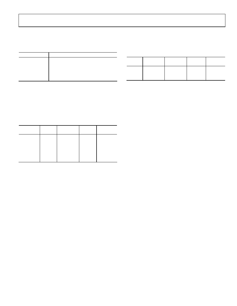
Table 30. Settings for Routing VCO Divider Input Directly
to LVPECL Outputs
Register Setting
Selection
0x1E1[1:0] = 00b
CLK is the source; VCO divider selected
0x1E1[1:0] = 10b
VCO is the source; VCO divider selected
0x192[1] = 1b
Direct to OUT0 and OUT1 outputs
0x195[1] = 1b
Direct to OUT2 and OUT3 outputs
0x198[1] = 1b
Direct to OUT4 and OUT5 outputs
Clock Frequency Division
The total frequency division is a combination of the VCO
divider (when used) and the channel divider. When the VCO
divider is used, the total division from the VCO or CLK to the
output is the product of the VCO divider (2, 3, 4, 5, 6) and the
division of the channel divider. Table 31 indicates how the
frequency division for a channel is set.
Table 31. Frequency Division for Divider 0 to Divider 2
CLK or VCO
Selected
VCO
Divider
Channel
Divider
Direct to
Output
Frequency
Division
CLK/VCO
2 to 6
1 (bypassed)
Yes
1
CLK/VCO
2 to 6
1 (bypassed)
No
(2 to 6) × (1)
CLK/VCO
2 to 6
2 to 32
No
(2 to 6) ×
(2 to 32)
CLK
Not used
1 (bypassed)
No
1
CLK
Not used
2 to 32
No
2 to 32
The channel dividers feeding the LVPECL output drivers
contain one 2-to-32 frequency divider. This divider provides for
division by 2 to 32. Division by 1 is accomplished by bypassing
the divider. The dividers also provide for a programmable duty
cycle, with optional duty-cycle correction when the divide ratio
is odd. A phase offset or delay in increments of the input clock
cycle is selectable. The channel dividers operate with a signal at
their inputs up to 1600 MHz. The features and settings of the
dividers are selected by programming the appropriate setup
VCO Divider
The VCO divider provides frequency division between the
internal VCO or the external CLK input and the clock
distribution channel dividers. The VCO divider can be set
to divide by 2, 3, 4, 5, or 6 (see Table 47, Register 0x1E0[2:0]).
Channel Dividers—LVPECL Outputs
Each pair of LVPECL outputs is driven by a channel divider.
There are three channel dividers (0, 1, and 2) driving a total
of six LVPECL outputs (OUT0 to OUT5). Table 32 gives the
register locations used for setting the division and other functions
of these dividers. The division is set by the values of M and N.
The divider can be bypassed (equivalent to divide-by-1, divider
circuit is powered down) by setting the bypass bit. The duty-
cycle correction can be enabled or disabled according to the
setting of the DCCOFF bits.
Divider
Low Cycles
M
High Cycles
N
Bypass
DCCOFF
0
0x190[7:4]
0x190[3:0]
0x191[7]
0x192[0]
1
0x193[7:4]
0x193[3:0]
0x194[7]
0x195[0]
2
0x196[7:4]
0x196[3:0]
0x197[7]
0x198[0]
1 Note that the value stored in the register = # of cycles minus 1.
Channel Frequency Division (0, 1, and 2)
For each channel (where the channel number is x: 0, 1, or 2),
the frequency division, DX, is set by the values of M and N
(four bits each, representing Decimal 0 to Decimal 15), where
Number of Low Cycles = M + 1
Number of High Cycles = N + 1
The cycles are cycles of the clock signal currently routed to the
input of the channel dividers (VCO divider out or CLK).
When a divider is bypassed, DX = 1.
Otherwise, DX = (N + 1) + (M + 1) = N + M + 2. This allows
each channel divider to divide by any integer from 2 to 32.
Duty Cycle and Duty-Cycle Correction (0, 1, and 2)
The duty cycle of the clock signal at the output of a channel is
a result of some or all of the following conditions:
What are the M and N values for the channel?
Is the DCC enabled?
Is the VCO divider used?
What is the CLK input duty cycle? (The internal VCO has
a 50% duty cycle.)
The DCC function is enabled by default for each channel divider.
However, the DCC function can be disabled individually for
each channel divider by setting the DCCOFF bit for that channel.
Certain M and N values for a channel divider result in a non-50%
duty cycle. A non-50% duty cycle can also result with an even
division, if M ≠ N. The duty-cycle correction function
automatically corrects non-50% duty cycles at the channel
divider output to 50% duty cycle. Duty-cycle correction
requires the following channel divider conditions:
An even division must be set as M = N.
An odd division must be set as M = N + 1.
When not bypassed or corrected by the DCC function, the duty
cycle of each channel divider output is the numerical value of
(N + 1)/(N + M + 2), expressed as a percentage (%).
相关PDF资料 |
PDF描述 |
|---|---|
| AD9518-4ABCPZ-RL7 | IC CLOCK GEN 6CH 1.8GHZ 48LFCSP |
| AD9520-0BCPZ-REEL7 | IC CLOCK GEN 2.8GHZ VCO 64LFCSP |
| AD9520-1BCPZ | IC CLOCK GEN 2.5GHZ VCO 64LFCSP |
| AD9520-2BCPZ | IC CLOCK GEN 2.2GHZ VCO 64LFCSP |
| AD9520-3BCPZ-REEL7 | IC CLOCK GEN 2GHZ VCO 64LFCSP |
相关代理商/技术参数 |
参数描述 |
|---|---|
| AD9518-3ABCPZ-RL7 | 功能描述:IC CLOCK GEN 6CH 2GHZ 48LFCSP RoHS:是 类别:集成电路 (IC) >> 时钟/计时 - 时钟发生器,PLL,频率合成器 系列:- 标准包装:2,000 系列:- 类型:PLL 时钟发生器 PLL:带旁路 输入:LVCMOS,LVPECL 输出:LVCMOS 电路数:1 比率 - 输入:输出:2:11 差分 - 输入:输出:是/无 频率 - 最大:240MHz 除法器/乘法器:是/无 电源电压:3.135 V ~ 3.465 V 工作温度:0°C ~ 70°C 安装类型:表面贴装 封装/外壳:32-LQFP 供应商设备封装:32-TQFP(7x7) 包装:带卷 (TR) |
| AD9518-3A-PCBZ | 制造商:AD 制造商全称:Analog Devices 功能描述:6-Output Clock Generator with 6-Output Clock Generator with |
| AD9518-3BCPZ | 制造商:Rochester Electronics LLC 功能描述: 制造商:Analog Devices 功能描述: |
| AD9518-3BCPZ-REEL7 | 制造商:Analog Devices 功能描述:Clock Generator 48-Pin LFCSP EP T/R |
| AD9518-4 | 制造商:AD 制造商全称:Analog Devices 功能描述:6-Output Clock Generator with Integrated 1.6 GHz VCO |
发布紧急采购,3分钟左右您将得到回复。