- 您现在的位置:买卖IC网 > PDF目录1987 > AD9520-5BCPZ-REEL7 (Analog Devices Inc)IC CLOCK GEN EXT VCO 64LFCSP PDF资料下载
参数资料
| 型号: | AD9520-5BCPZ-REEL7 |
| 厂商: | Analog Devices Inc |
| 文件页数: | 10/76页 |
| 文件大小: | 0K |
| 描述: | IC CLOCK GEN EXT VCO 64LFCSP |
| 设计资源: | Synchronizing Multiple AD9910 1 GSPS Direct Digital Synthesizers (CN0121) Phase Coherent FSK Modulator (CN0186) |
| 标准包装: | 750 |
| 类型: | 时钟发生器,扇出配送 |
| PLL: | 是 |
| 输入: | CMOS,LVDS,LVPECL |
| 输出: | CMOS,LVPECL |
| 电路数: | 1 |
| 比率 - 输入:输出: | 2:12,2:24 |
| 差分 - 输入:输出: | 是/是 |
| 频率 - 最大: | 2.4GHz |
| 除法器/乘法器: | 是/无 |
| 电源电压: | 3.135 V ~ 3.465 V |
| 工作温度: | -40°C ~ 85°C |
| 安装类型: | 表面贴装 |
| 封装/外壳: | 64-VFQFN 裸露焊盘,CSP |
| 供应商设备封装: | 64-LFCSP-VQ(9x9) |
| 包装: | 带卷 (TR) |
第1页第2页第3页第4页第5页第6页第7页第8页第9页当前第10页第11页第12页第13页第14页第15页第16页第17页第18页第19页第20页第21页第22页第23页第24页第25页第26页第27页第28页第29页第30页第31页第32页第33页第34页第35页第36页第37页第38页第39页第40页第41页第42页第43页第44页第45页第46页第47页第48页第49页第50页第51页第52页第53页第54页第55页第56页第57页第58页第59页第60页第61页第62页第63页第64页第65页第66页第67页第68页第69页第70页第71页第72页第73页第74页第75页第76页
AD9520-5
Data Sheet
Rev. A | Page 18 of 76
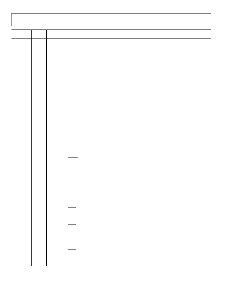
Pin No.
Input/
Output
Pin Type
Mnemonic
Description
15
I
3.3 V CMOS
CS
Serial Control Port Chip Select; Active Low. This pin has an internal 30 kΩ pull-up
resistor.
16
I
3.3 V CMOS
SCLK/SCL
Serial Control Port Clock Signal. This pin has an internal 30 kΩ pull-down resistor
in SPI mode but is high impedance in IC mode.
17
I/O
3.3 V CMOS
SDIO/SDA
Serial Control Port Bidirectional Serial Data In/Out.
18
O
3.3 V CMOS
SDO
Serial Control Port Unidirectional Serial Data Out.
19, 59
I
GND
Ground Pins.
20
I
Three-level
logic
SP1
Select SPI or IC as the serial interface port and select the IC slave address in IC
mode. Three-level logic. This pin is internally biased for the open logic level.
21
I
Three-level
logic
SP0
Select SPI or IC as the serial interface port and select the IC slave address in IC
mode. Three-level logic. This pin is internally biased for the open logic level.
22
I
3.3 V CMOS
EEPROM
Setting this pin high selects the register values stored in the internal EEPROM to be
loaded at reset and/or power-up. Setting this pin low causes the AD9520 to load
the hard-coded default register values at power-up/reset (unless Register 0xB02[1]
is used. See the Soft Reset via the Serial Port section). This pin has an internal 30 kΩ
pull-down resistor. Note that, to guarantee proper loading of the EEPROM during
startup, a high-low-high pulse on the RESET pin should occur after the power supply
has stabilized.
23
I
3.3 V CMOS
RESET
Chip Reset, Active Low. This pin has an internal 30 kΩ pull-up resistor.
24
I
3.3 V CMOS
PD
Chip Power-Down, Active Low. This pin has an internal 30 kΩ pull-up resistor.
25
O
LVPECL or
CMOS
OUT9 (OUT9A)
Clock Output. This pin can be configured as one side of a differential LVPECL
output or as a single-ended CMOS output.
26
O
LVPECL or
CMOS
OUT9 (OUT9B)
Clock Output. This pin can be configured as one side of a differential LVPECL
output or as a single-ended CMOS output.
27, 35,
46, 54
I
Power
VS_DRV
Output Driver Power Supply Pins. As a group, these pins can be set to either 2.5 V
or 3.3 V. All four pins must be set to the same voltage.
28
O
LVPECL or
CMOS
OUT10 (OUT10A)
Clock Output. This pin can be configured as one side of a differential LVPECL
output or as a single-ended CMOS output.
29
O
LVPECL or
CMOS
OUT10 (OUT10B)
Clock Output. This pin can be configured as one side of a differential LVPECL
output or as a single-ended CMOS output.
30
O
LVPECL or
CMOS
OUT11 (OUT11A)
Clock Output. This pin can be configured as one side of a differential LVPECL
output or as a single-ended CMOS output.
31
O
LVPECL or
CMOS
OUT11 (OUT11B)
Clock Output. This pin can be configured as one side of a differential LVPECL
output or as a single-ended CMOS output.
33
O
LVPECL or
CMOS
OUT6 (OUT6A)
Clock Output. This pin can be configured as one side of a differential LVPECL
output or as a single-ended CMOS output.
34
O
LVPECL or
CMOS
OUT6 (OUT6B)
Clock Output. This pin can be configured as one side of a differential LVPECL
output or as a single-ended CMOS output.
36
O
LVPECL or
CMOS
OUT7 (OUT7A)
Clock Output. This pin can be configured as one side of a differential LVPECL
output or as a single-ended CMOS output.
37
O
LVPECL or
CMOS
OUT7 (OUT7B)
Clock Output. This pin can be configured as one side of a differential LVPECL
output or as a single-ended CMOS output.
38
O
LVPECL or
CMOS
OUT8 (OUT8A)
Clock Output. This pin can be configured as one side of a differential LVPECL
output or as a single-ended CMOS output.
39
O
LVPECL or
CMOS
OUT8 (OUT8B)
Clock Output. This pin can be configured as one side of a differential LVPECL
output or as a single-ended CMOS output.
42
O
LVPECL or
CMOS
OUT5 (OUT5B)
Clock Output. This pin can be configured as one side of a differential LVPECL
output or as a single-ended CMOS output.
43
O
LVPECL or
CMOS
OUT5 (OUT5A)
Clock Output. This pin can be configured as one side of a differential LVPECL
output or as a single-ended CMOS output.
44
O
LVPECL or
CMOS
OUT4 (OUT4B)
Clock Output. This pin can be configured as one side of a differential LVPECL
output or as a single-ended CMOS output.
45
O
LVPECL or
CMOS
OUT4 (OUT4A)
Clock Output. This pin can be configured as one side of a differential LVPECL
output or as a single-ended CMOS output.
相关PDF资料 |
PDF描述 |
|---|---|
| AD9522-0BCPZ-REEL7 | IC CLOCK GEN 2.8GHZ VCO 64LFCSP |
| AD9522-1BCPZ-REEL7 | IC CLOCK GEN 2.5GHZ VCO 64LFCSP |
| AD9522-2BCPZ | IC CLOCK GEN 2.2GHZ VCO 64LFCSP |
| AD9522-3BCPZ-REEL7 | IC CLOCK GEN 2GHZ VCO 64LFCSP |
| AD9522-4BCPZ-REEL7 | IC CLOCK GEN 1.6GHZ VCO 64LFCSP |
相关代理商/技术参数 |
参数描述 |
|---|---|
| AD9521JH | 制造商:未知厂家 制造商全称:未知厂家 功能描述:Log/Antilog Amplifier |
| AD9521KH | 制造商:未知厂家 制造商全称:未知厂家 功能描述:Log/Antilog Amplifier |
| AD9521SE | 制造商:未知厂家 制造商全称:未知厂家 功能描述:Log/Antilog Amplifier |
| AD9521SH | 制造商:未知厂家 制造商全称:未知厂家 功能描述:Log/Antilog Amplifier |
| AD9521TE | 制造商:未知厂家 制造商全称:未知厂家 功能描述:Log/Antilog Amplifier |
发布紧急采购,3分钟左右您将得到回复。