- 您现在的位置:买卖IC网 > PDF目录1987 > AD9520-5BCPZ-REEL7 (Analog Devices Inc)IC CLOCK GEN EXT VCO 64LFCSP PDF资料下载
参数资料
| 型号: | AD9520-5BCPZ-REEL7 |
| 厂商: | Analog Devices Inc |
| 文件页数: | 5/76页 |
| 文件大小: | 0K |
| 描述: | IC CLOCK GEN EXT VCO 64LFCSP |
| 设计资源: | Synchronizing Multiple AD9910 1 GSPS Direct Digital Synthesizers (CN0121) Phase Coherent FSK Modulator (CN0186) |
| 标准包装: | 750 |
| 类型: | 时钟发生器,扇出配送 |
| PLL: | 是 |
| 输入: | CMOS,LVDS,LVPECL |
| 输出: | CMOS,LVPECL |
| 电路数: | 1 |
| 比率 - 输入:输出: | 2:12,2:24 |
| 差分 - 输入:输出: | 是/是 |
| 频率 - 最大: | 2.4GHz |
| 除法器/乘法器: | 是/无 |
| 电源电压: | 3.135 V ~ 3.465 V |
| 工作温度: | -40°C ~ 85°C |
| 安装类型: | 表面贴装 |
| 封装/外壳: | 64-VFQFN 裸露焊盘,CSP |
| 供应商设备封装: | 64-LFCSP-VQ(9x9) |
| 包装: | 带卷 (TR) |
第1页第2页第3页第4页当前第5页第6页第7页第8页第9页第10页第11页第12页第13页第14页第15页第16页第17页第18页第19页第20页第21页第22页第23页第24页第25页第26页第27页第28页第29页第30页第31页第32页第33页第34页第35页第36页第37页第38页第39页第40页第41页第42页第43页第44页第45页第46页第47页第48页第49页第50页第51页第52页第53页第54页第55页第56页第57页第58页第59页第60页第61页第62页第63页第64页第65页第66页第67页第68页第69页第70页第71页第72页第73页第74页第75页第76页
Data Sheet
AD9520-5
Rev. A | Page 13 of 76
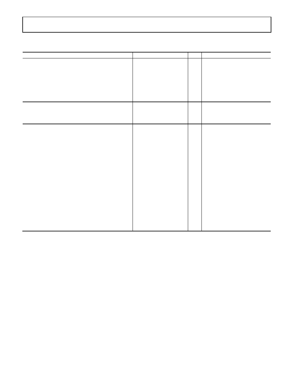
SERIAL CONTROL PORT—IC MODE
Table 11.
Parameter
Min
Typ
Max
Unit
Test Conditions/Comments
SDA, SCL (WHEN INPUTTING DATA)
Input Logic 1 Voltage
0.7 × VS
V
Input Logic 0 Voltage
0.3 × VS
V
Input Current with an Input Voltage Between 0.1 × VS
and 0.9 × VS
10
+10
A
Hysteresis of Schmitt Trigger Inputs
0.015 × VS
V
Pulse Width of Spikes That Must Be Suppressed by the
Input Filter, tSPIKE
50
ns
SDA (WHEN OUTPUTTING DATA)
Output Logic 0 Voltage at 3 mA Sink Current
0.4
V
Output Fall Time from VIHMIN to VILMAX with a Bus
Capacitance from 10 pF to 400 pF
20 + 0.1 Cb
250
ns
Cb = capacitance of one bus line in pF
TIMING
Note that all I2C timing values are
referred to VIHMIN (0.3 × VS) and
VILMAX levels (0.7 × VS)
Clock Rate (SCL, fI2C)
400
kHz
Bus Free Time Between a Stop and Start Condition, tIDLE
1.3
s
Setup Time for a Repeated Start Condition, tSET; STR
0.6
s
Hold Time (Repeated) Start Condition, tHLD; STR
0.6
s
After this period, the first clock pulse
is generated
Setup Time for Stop Condition, tSET; STP
0.6
s
Low Period of the SCL Clock, tLOW
1.3
s
High Period of the SCL Clock, tHIGH
0.6
s
SCL, SDA Rise Time, tRISE
20 + 0.1 Cb
300
ns
SCL, SDA Fall Time, tFALL
20 + 0.1 Cb
300
ns
Data Setup Time, tSET; DAT
120
ns
This is a minor deviation from the
original IC specification of 100 ns
minimum
Data Hold Time, tHLD; DAT
140
880
ns
This is a minor deviation from the
original IC specification of 0 ns
Capacitive Load for Each Bus Line, Cb
400
pF
1
According to the original I2C specification, an I2C master must also provide a minimum hold time of 300 ns for the SDA signal to bridge the undefined region of the SCL
falling edge.
相关PDF资料 |
PDF描述 |
|---|---|
| AD9522-0BCPZ-REEL7 | IC CLOCK GEN 2.8GHZ VCO 64LFCSP |
| AD9522-1BCPZ-REEL7 | IC CLOCK GEN 2.5GHZ VCO 64LFCSP |
| AD9522-2BCPZ | IC CLOCK GEN 2.2GHZ VCO 64LFCSP |
| AD9522-3BCPZ-REEL7 | IC CLOCK GEN 2GHZ VCO 64LFCSP |
| AD9522-4BCPZ-REEL7 | IC CLOCK GEN 1.6GHZ VCO 64LFCSP |
相关代理商/技术参数 |
参数描述 |
|---|---|
| AD9521JH | 制造商:未知厂家 制造商全称:未知厂家 功能描述:Log/Antilog Amplifier |
| AD9521KH | 制造商:未知厂家 制造商全称:未知厂家 功能描述:Log/Antilog Amplifier |
| AD9521SE | 制造商:未知厂家 制造商全称:未知厂家 功能描述:Log/Antilog Amplifier |
| AD9521SH | 制造商:未知厂家 制造商全称:未知厂家 功能描述:Log/Antilog Amplifier |
| AD9521TE | 制造商:未知厂家 制造商全称:未知厂家 功能描述:Log/Antilog Amplifier |
发布紧急采购,3分钟左右您将得到回复。