- 您现在的位置:买卖IC网 > PDF目录1987 > AD9522-0BCPZ-REEL7 (Analog Devices Inc)IC CLOCK GEN 2.8GHZ VCO 64LFCSP PDF资料下载
参数资料
| 型号: | AD9522-0BCPZ-REEL7 |
| 厂商: | Analog Devices Inc |
| 文件页数: | 35/84页 |
| 文件大小: | 0K |
| 描述: | IC CLOCK GEN 2.8GHZ VCO 64LFCSP |
| 标准包装: | 750 |
| 类型: | 时钟发生器,扇出配送 |
| PLL: | 是 |
| 输入: | CMOS,LVDS,LVPECL |
| 输出: | CMOS,LVDS |
| 电路数: | 1 |
| 比率 - 输入:输出: | 2:12,2:24 |
| 差分 - 输入:输出: | 是/是 |
| 频率 - 最大: | 2.95GHz |
| 除法器/乘法器: | 是/无 |
| 电源电压: | 3.135 V ~ 3.465 V |
| 工作温度: | -40°C ~ 85°C |
| 安装类型: | 表面贴装 |
| 封装/外壳: | 64-VFQFN 裸露焊盘,CSP |
| 供应商设备封装: | 64-LFCSP-VQ(9x9) |
| 包装: | 带卷 (TR) |
第1页第2页第3页第4页第5页第6页第7页第8页第9页第10页第11页第12页第13页第14页第15页第16页第17页第18页第19页第20页第21页第22页第23页第24页第25页第26页第27页第28页第29页第30页第31页第32页第33页第34页当前第35页第36页第37页第38页第39页第40页第41页第42页第43页第44页第45页第46页第47页第48页第49页第50页第51页第52页第53页第54页第55页第56页第57页第58页第59页第60页第61页第62页第63页第64页第65页第66页第67页第68页第69页第70页第71页第72页第73页第74页第75页第76页第77页第78页第79页第80页第81页第82页第83页第84页
AD9522-0
Rev. 0 | Page 40 of 84
After leaving holdover, the loop then reacquires lock and the
LD pin must go high (if 0x01D[3] = 1) before it can reenter
holdover.
The holdover function always responds to the state of the
currently selected reference (0x01C). If the loop loses lock
during a reference switchover (see the Reference Switchover
section), holdover is triggered briefly until the next reference
clock edge at the PFD.
The following registers affect the automatic/internal holdover
function:
0x018[6:5]—lock detect counter. This changes how many
consecutive PFD cycles with edges inside the lock detect
window are required for the DLD indicator to indicate
lock. This impacts the time required before the LD pin can
begin to charge as well as the delay from the end of a
holdover event until the holdover function can be
reengaged.
0x018[3]—disable digital lock detect. This bit must be set
to a 0 to enable the DLD circuit. Internal/automatic
holdover does not operate correctly without the DLD
function enabled.
0x01A[5:0]—lock detect pin control. Set this to 000100b to
put it in the current source lock detect mode if using the
LD pin comparator. Load the LD pin with a capacitor of an
appropriate value.
0x01D[3]—LD pin comparator enable. 1 = enable; 0 =
disable. When disabled, the holdover function always
senses the LD pin as high.
0x01D[1]—external holdover control.
0x01D[0]—holdover enable. If holdover is disabled, both
external and automatic/internal holdover are disabled.
In the following example, automatic holdover is configured with
Automatic reference switchover, prefer REF1.
Digital lock detect: five PFD cycles, high range window.
Automatic holdover using the LD pin comparator.
The following registers are set (in addition to the normal PLL
registers):
0x018[6:5] = 00b; lock detect counter = five cycles.
0x018[4] = 0b; digital lock detect window = high range.
0x018[3] = 1b; disable DLD normal operation.
0x01A[5:0] = 000100b; program LD pin control to current
source lock detect mode.
0x01C[4] = 1b; enable automatic switchover.
0x01C[3] = 0b; prefer REF1.
0x01C[2:1] = 11b; enable REF1 and REF2 input buffers.
0x01D[3] = 1b; enable LD pin comparator.
0x01D[1] = 0b; disable external holdover mode and use
automatic/internal holdover mode.
0x01D[0] = 1b; enable holdover.
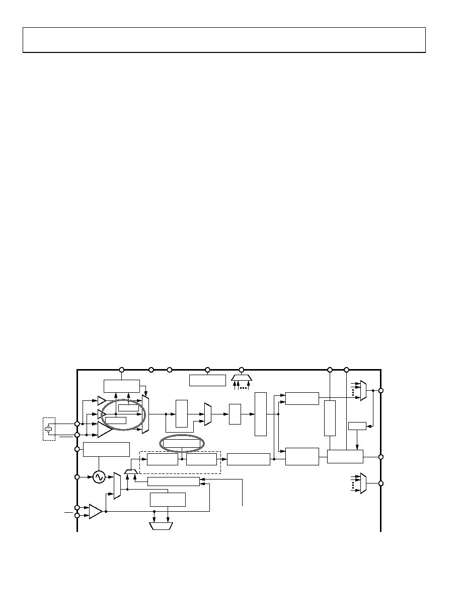
Frequency Status Monitors
The AD9522 contains three frequency status monitors that are
used to indicate if the PLL reference (or references in the case of
single-ended mode) and the VCO have fallen below a threshold
frequency. A diagram showing their location in the PLL is
shown in Figure 48.
The PLL reference monitors have two threshold frequencies:
normal and extended (see Table 17). The reference frequency
monitor thresholds are selected in 0x01F.
PROGRAMMABLE
N DELAY
CLK
REF1
REF2
BUF
STATUS
R
DI
V
IDE
R
CL
O
CK
DO
UB
L
E
R
VCO STATUS
P
R
O
G
RA
M
ABL
E
R
DE
L
AY
REFERENCE
SWITCHOVER
REF_SEL
CPRSET VCP
VS
GND
RSET
DISTRIBUTION
REFERENCE
REFMON
CP
STATUS
LD
P, P + 1
PRESCALER
A/B
COUNTERS
N DIVIDER
BYPASS
LF
LOW DROPOUT
REGULATOR (LDO)
PHASE
FREQUENCY
DETECTOR
LOCK
DETECT
CHARGE
PUMP
PL
L
RE
F
E
RE
NCE
HOLD
0
1
DIVIDE BY 1,
2, 3, 4, 5, OR 6
ZERO DELAY BLOCK
FROM CHANNEL
DIVIDER 0
REFIN
OPTIONAL
REFIN
07
21
9-
0
70
Figure 48. Reference and VCO Status Monitors
相关PDF资料 |
PDF描述 |
|---|---|
| AD9522-1BCPZ-REEL7 | IC CLOCK GEN 2.5GHZ VCO 64LFCSP |
| AD9522-2BCPZ | IC CLOCK GEN 2.2GHZ VCO 64LFCSP |
| AD9522-3BCPZ-REEL7 | IC CLOCK GEN 2GHZ VCO 64LFCSP |
| AD9522-4BCPZ-REEL7 | IC CLOCK GEN 1.6GHZ VCO 64LFCSP |
| AD9522-5BCPZ | IC CLOCK GEN 2.4GHZ 64LFCSP |
相关代理商/技术参数 |
参数描述 |
|---|---|
| AD9522-1 | 制造商:AD 制造商全称:Analog Devices 功能描述:12 LVDS/24 CMOS Output Clock Generator with Integrated 2.4 GHz VCO |
| AD9522-1/PCBZ | 功能描述:BOARD EVAL FOR AD9522-1 CLK GEN RoHS:是 类别:编程器,开发系统 >> 评估演示板和套件 系列:- 标准包装:1 系列:- 主要目的:电信,线路接口单元(LIU) 嵌入式:- 已用 IC / 零件:IDT82V2081 主要属性:T1/J1/E1 LIU 次要属性:- 已供物品:板,电源,线缆,CD 其它名称:82EBV2081 |
| AD9522-1BCPZ | 功能描述:IC CLOCK GEN 2.5GHZ VCO 64LFCSP RoHS:是 类别:集成电路 (IC) >> 时钟/计时 - 时钟发生器,PLL,频率合成器 系列:- 标准包装:1,000 系列:Precision Edge® 类型:时钟/频率合成器 PLL:无 输入:CML,PECL 输出:CML 电路数:1 比率 - 输入:输出:2:1 差分 - 输入:输出:是/是 频率 - 最大:10.7GHz 除法器/乘法器:无/无 电源电压:2.375 V ~ 3.6 V 工作温度:-40°C ~ 85°C 安装类型:表面贴装 封装/外壳:16-VFQFN 裸露焊盘,16-MLF? 供应商设备封装:16-MLF?(3x3) 包装:带卷 (TR) 其它名称:SY58052UMGTRSY58052UMGTR-ND |
| AD9522-1BCPZ-REEL7 | 功能描述:IC CLOCK GEN 2.5GHZ VCO 64LFCSP RoHS:是 类别:集成电路 (IC) >> 时钟/计时 - 时钟发生器,PLL,频率合成器 系列:- 标准包装:2,000 系列:- 类型:PLL 时钟发生器 PLL:带旁路 输入:LVCMOS,LVPECL 输出:LVCMOS 电路数:1 比率 - 输入:输出:2:11 差分 - 输入:输出:是/无 频率 - 最大:240MHz 除法器/乘法器:是/无 电源电压:3.135 V ~ 3.465 V 工作温度:0°C ~ 70°C 安装类型:表面贴装 封装/外壳:32-LQFP 供应商设备封装:32-TQFP(7x7) 包装:带卷 (TR) |
| AD9522-2 | 制造商:AD 制造商全称:Analog Devices 功能描述:12 LVDS/24 CMOS Output Clock Generator with Integrated 2.2 GHz VCO |
发布紧急采购,3分钟左右您将得到回复。