- 您现在的位置:买卖IC网 > PDF目录1987 > AD9522-0BCPZ-REEL7 (Analog Devices Inc)IC CLOCK GEN 2.8GHZ VCO 64LFCSP PDF资料下载
参数资料
| 型号: | AD9522-0BCPZ-REEL7 |
| 厂商: | Analog Devices Inc |
| 文件页数: | 38/84页 |
| 文件大小: | 0K |
| 描述: | IC CLOCK GEN 2.8GHZ VCO 64LFCSP |
| 标准包装: | 750 |
| 类型: | 时钟发生器,扇出配送 |
| PLL: | 是 |
| 输入: | CMOS,LVDS,LVPECL |
| 输出: | CMOS,LVDS |
| 电路数: | 1 |
| 比率 - 输入:输出: | 2:12,2:24 |
| 差分 - 输入:输出: | 是/是 |
| 频率 - 最大: | 2.95GHz |
| 除法器/乘法器: | 是/无 |
| 电源电压: | 3.135 V ~ 3.465 V |
| 工作温度: | -40°C ~ 85°C |
| 安装类型: | 表面贴装 |
| 封装/外壳: | 64-VFQFN 裸露焊盘,CSP |
| 供应商设备封装: | 64-LFCSP-VQ(9x9) |
| 包装: | 带卷 (TR) |
第1页第2页第3页第4页第5页第6页第7页第8页第9页第10页第11页第12页第13页第14页第15页第16页第17页第18页第19页第20页第21页第22页第23页第24页第25页第26页第27页第28页第29页第30页第31页第32页第33页第34页第35页第36页第37页当前第38页第39页第40页第41页第42页第43页第44页第45页第46页第47页第48页第49页第50页第51页第52页第53页第54页第55页第56页第57页第58页第59页第60页第61页第62页第63页第64页第65页第66页第67页第68页第69页第70页第71页第72页第73页第74页第75页第76页第77页第78页第79页第80页第81页第82页第83页第84页
AD9522-0
Rev. 0 | Page 43 of 84
MODE 0 (INTERNAL VCO MODE)
CLK
LF
0
1
DIVIDE BY 1,
2, 3, 4, 5, OR 6
CLOCK
DISTRI-
BUTION
PLL
DISTRIBUTION
CLOCK
MODE 1 (CLOCK DISTRIBUTION MODE)
DISTRIBUTION
CLOCK
MODE 2 (HF CLOCK DISTRIBUTION MODE)
CLK
LF
0
1
DIVIDE BY 1,
2, 3, 4, 5, OR 6
CLOCK
DISTRI-
BUTION
PLL
CLK
LF
0
1
DIVIDE BY 1,
2, 3, 4, 5, OR 6
CLOCK
DISTRI-
BUTION
PLL
DISTRIBUTION
CLOCK
07
21
9-
05
4
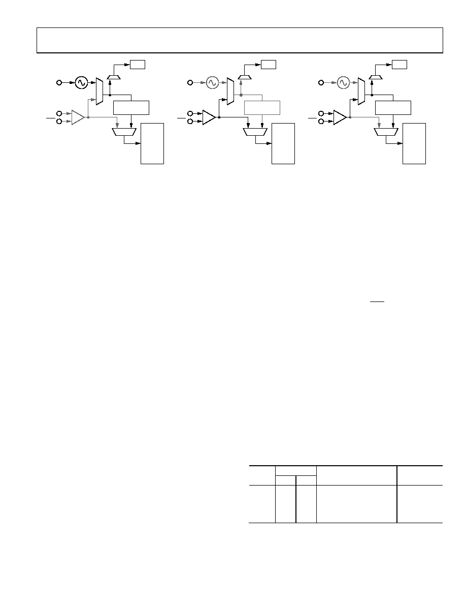
Figure 50. Simplified Diagram of the Three Clock Distribution Operation Modes
CLOCK DISTRIBUTION
A clock channel consists of three LVDS clock outputs or six
CMOS clock outputs that share a common divider. A clock
output consists of the drivers that connect to the output pins.
The clock outputs have either LVDS or CMOS at the pins.
The AD9522 has four clock channels. Each channel has its own
programmable divider that divides the clock frequency applied
to its input. The channel dividers can divide by any integer
from 1 to 32.
The AD9522 features a VCO divider that divides the VCO output
by 1, 2, 3, 4, 5, or 6 before going to the individual channel dividers.
The VCO divider has two purposes. The first is to limit the
maximum input frequency of the channel dividers to 1.6 GHz.
The other is to allow the AD9522 to generate even lower
frequencies than would be possible with only a simple post divider.
External clock signals connected to the CLK input can also use
the VCO divider.
The channel dividers allow for a selection of various duty cycles,
depending on the currently set division. That is, for any specific
division, D, the output of the divider can be set to high for N + 1
input clock cycles and low for M + 1 input clock cycles (where
D = N + M + 2). For example, a divide-by-5 can be high for one
divider input cycle and low for four cycles, or a divide-by-5 can
be high for three divider input cycles and low for two cycles.
Other combinations are also possible.
The channel dividers include a duty-cycle correction function
that can be disabled. In contrast to the selectable duty cycle
just described, this function can correct a non-50% duty cycle
caused by an odd division. However, this requires that the
division be set by M = N + 1.
In addition, the channel dividers allow a coarse phase offset or
delay to be set. Depending on the division selected, the output
can be delayed by up to 15 input clock cycles. For example, if
the frequency at the input of the channel divider is 1 GHz, the
channel divider output can be delayed by up to 15 ns. The
divider outputs can also be set to start high or to start low.
Operation Modes
There are three clock distribution operating modes, and these
are shown in Figure 50. One of these modes uses the internal
VCO, whereas the other two modes bypass the internal VCO
and use the signal provided on the CLK/CLK pins.
In Mode 0 (internal VCO mode), there are two signal paths
available. In the first path, the VCO signal is sent to the VCO
divider and then to the individual channel dividers. In the
second path, the user bypasses the VCO and channel dividers
and sends the VCO signal directly to the drivers.
When CLK is selected as the source, it is not necessary to use the
VCO divider if the CLK frequency is less than the maximum
channel divider input frequency (1600 MHz); otherwise, the
VCO divider must be used to reduce the frequency going to
the channel dividers.
Table 31 shows how the VCO, CLK, and VCO divider are selected.
0x1E1[1:0] selects the channel divider source and determines
whether the VCO divider is used. It is not possible to select the
VCO without using the VCO divider.
Table 31. Operation Modes
0x1E1
Mode
[1]
[0]
Channel Divider Source
VCO Divider
2
0
CLK
Used
1
0
1
CLK
Not used
0
1
0
VCO
Used
1
Not allowed
相关PDF资料 |
PDF描述 |
|---|---|
| AD9522-1BCPZ-REEL7 | IC CLOCK GEN 2.5GHZ VCO 64LFCSP |
| AD9522-2BCPZ | IC CLOCK GEN 2.2GHZ VCO 64LFCSP |
| AD9522-3BCPZ-REEL7 | IC CLOCK GEN 2GHZ VCO 64LFCSP |
| AD9522-4BCPZ-REEL7 | IC CLOCK GEN 1.6GHZ VCO 64LFCSP |
| AD9522-5BCPZ | IC CLOCK GEN 2.4GHZ 64LFCSP |
相关代理商/技术参数 |
参数描述 |
|---|---|
| AD9522-1 | 制造商:AD 制造商全称:Analog Devices 功能描述:12 LVDS/24 CMOS Output Clock Generator with Integrated 2.4 GHz VCO |
| AD9522-1/PCBZ | 功能描述:BOARD EVAL FOR AD9522-1 CLK GEN RoHS:是 类别:编程器,开发系统 >> 评估演示板和套件 系列:- 标准包装:1 系列:- 主要目的:电信,线路接口单元(LIU) 嵌入式:- 已用 IC / 零件:IDT82V2081 主要属性:T1/J1/E1 LIU 次要属性:- 已供物品:板,电源,线缆,CD 其它名称:82EBV2081 |
| AD9522-1BCPZ | 功能描述:IC CLOCK GEN 2.5GHZ VCO 64LFCSP RoHS:是 类别:集成电路 (IC) >> 时钟/计时 - 时钟发生器,PLL,频率合成器 系列:- 标准包装:1,000 系列:Precision Edge® 类型:时钟/频率合成器 PLL:无 输入:CML,PECL 输出:CML 电路数:1 比率 - 输入:输出:2:1 差分 - 输入:输出:是/是 频率 - 最大:10.7GHz 除法器/乘法器:无/无 电源电压:2.375 V ~ 3.6 V 工作温度:-40°C ~ 85°C 安装类型:表面贴装 封装/外壳:16-VFQFN 裸露焊盘,16-MLF? 供应商设备封装:16-MLF?(3x3) 包装:带卷 (TR) 其它名称:SY58052UMGTRSY58052UMGTR-ND |
| AD9522-1BCPZ-REEL7 | 功能描述:IC CLOCK GEN 2.5GHZ VCO 64LFCSP RoHS:是 类别:集成电路 (IC) >> 时钟/计时 - 时钟发生器,PLL,频率合成器 系列:- 标准包装:2,000 系列:- 类型:PLL 时钟发生器 PLL:带旁路 输入:LVCMOS,LVPECL 输出:LVCMOS 电路数:1 比率 - 输入:输出:2:11 差分 - 输入:输出:是/无 频率 - 最大:240MHz 除法器/乘法器:是/无 电源电压:3.135 V ~ 3.465 V 工作温度:0°C ~ 70°C 安装类型:表面贴装 封装/外壳:32-LQFP 供应商设备封装:32-TQFP(7x7) 包装:带卷 (TR) |
| AD9522-2 | 制造商:AD 制造商全称:Analog Devices 功能描述:12 LVDS/24 CMOS Output Clock Generator with Integrated 2.2 GHz VCO |
发布紧急采购,3分钟左右您将得到回复。