- 您现在的位置:买卖IC网 > PDF目录1987 > AD9522-0BCPZ-REEL7 (Analog Devices Inc)IC CLOCK GEN 2.8GHZ VCO 64LFCSP PDF资料下载
参数资料
| 型号: | AD9522-0BCPZ-REEL7 |
| 厂商: | Analog Devices Inc |
| 文件页数: | 75/84页 |
| 文件大小: | 0K |
| 描述: | IC CLOCK GEN 2.8GHZ VCO 64LFCSP |
| 标准包装: | 750 |
| 类型: | 时钟发生器,扇出配送 |
| PLL: | 是 |
| 输入: | CMOS,LVDS,LVPECL |
| 输出: | CMOS,LVDS |
| 电路数: | 1 |
| 比率 - 输入:输出: | 2:12,2:24 |
| 差分 - 输入:输出: | 是/是 |
| 频率 - 最大: | 2.95GHz |
| 除法器/乘法器: | 是/无 |
| 电源电压: | 3.135 V ~ 3.465 V |
| 工作温度: | -40°C ~ 85°C |
| 安装类型: | 表面贴装 |
| 封装/外壳: | 64-VFQFN 裸露焊盘,CSP |
| 供应商设备封装: | 64-LFCSP-VQ(9x9) |
| 包装: | 带卷 (TR) |
第1页第2页第3页第4页第5页第6页第7页第8页第9页第10页第11页第12页第13页第14页第15页第16页第17页第18页第19页第20页第21页第22页第23页第24页第25页第26页第27页第28页第29页第30页第31页第32页第33页第34页第35页第36页第37页第38页第39页第40页第41页第42页第43页第44页第45页第46页第47页第48页第49页第50页第51页第52页第53页第54页第55页第56页第57页第58页第59页第60页第61页第62页第63页第64页第65页第66页第67页第68页第69页第70页第71页第72页第73页第74页当前第75页第76页第77页第78页第79页第80页第81页第82页第83页第84页
AD9522-0
Rev. 0 | Page 77 of 84
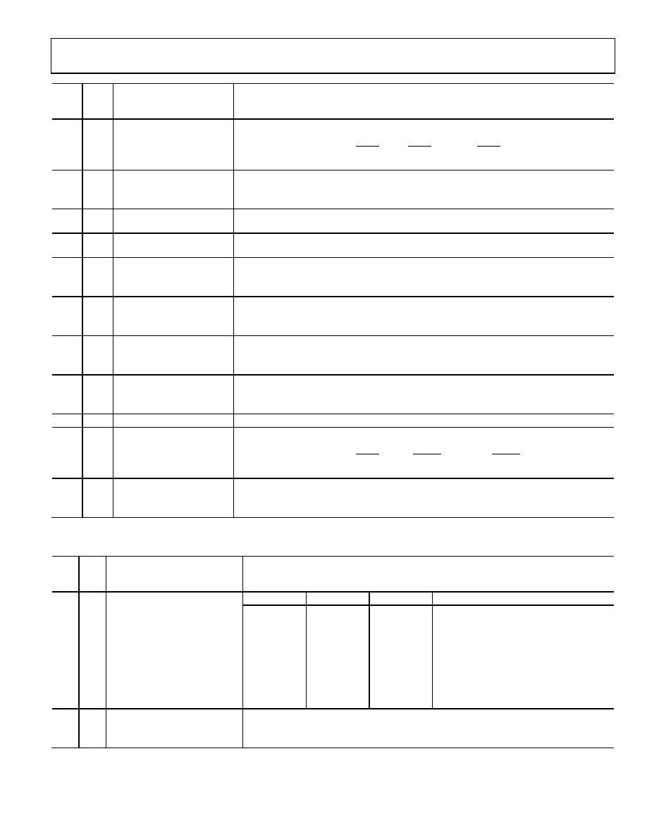
Reg.
Addr
(Hex) Bit(s) Name
Description
198
[2]
Channel 2 power-down
Channel 2 powers down.
[2] = 0; normal operation (default).
[2] = 1; powered down. (OUT6/OUT6, OUT7/OUT7, and OUT8/OUT8 are put into the high
impedance power-down mode by setting this bit.)
198
[0]
Disable Divider 2 DCC
Duty-cycle correction function.
[0] = 0; enable duty-cycle correction (default).
[0] = 1; disable duty-cycle correction.
199
[7:4]
Divider 3 low cycles
Number of clock cycles (minus 1) of the divider input during which the divider output stays
low. A value of 0x0 means the divider is low for one input clock cycle (default: 0x0).
199
[3:0]
Divider 3 high cycles
Number of clock cycles (minus 1) of the divider input during which the divider output stays
high. A value of 0x0 means the divider is high for one input clock cycle (default: 0x0).
19A
[7]
Divider 3 bypass
Bypasses and powers down the divider; routes input to divider output.
[7] = 0; use the divider (default).
[7] = 1; bypass the divider.
19A
[6]
Divider 3 ignore SYNC
Ignore SYNC.
[6] = 0; obey chip-level SYNC signal (default).
[6] = 1; ignore chip-level SYNC signal.
19A
[5]
Divider 3 force high
Forces divider output to high. This requires that ignore SYNC also be set.
[5] = 0; divider output forced to low (default).
[5] = 1; divider output forced to high.
19A
[4]
Divider 3 start high
Selects clock output to start high or start low.
[4] = 0; start low (default).
[4] = 1; start high.
19A
[3:0]
Divider 3 phase offset
Phase offset (default: 0x0).
19B
[2]
Channel 3 power-down
Channel 3 powers down.
[2] = 0; normal operation (default).
[2] = 1; powered down. (OUT9/OUT9, OUT10/OUT10, and OUT11/OUT11 are put into the high
impedance power-down mode by setting this bit.)
19B
[0]
Disable Divider 3 DCC
Duty-cycle correction function.
[0] = 0; enable duty-cycle correction (default).
[0] = 1; disable duty-cycle correction.
Table 55. VCO Divider and CLK Input
Reg.
Addr
(Hex) Bit(s) Name
Description
1E0
[2:0]
VCO divider
[2]
[1]
[0]
Divide
0
2 (default)
0
1
3
0
1
0
4
0
1
5
1
0
6
1
0
1
Output static
1
0
1 (bypass)
1
Output static
1E1
[4]
Power-down clock input section
Powers down the clock input section (including CLK buffer, VCO divider, and CLK tree).
[4] = 0; normal operation (default).
[4] = 1; power down.
相关PDF资料 |
PDF描述 |
|---|---|
| AD9522-1BCPZ-REEL7 | IC CLOCK GEN 2.5GHZ VCO 64LFCSP |
| AD9522-2BCPZ | IC CLOCK GEN 2.2GHZ VCO 64LFCSP |
| AD9522-3BCPZ-REEL7 | IC CLOCK GEN 2GHZ VCO 64LFCSP |
| AD9522-4BCPZ-REEL7 | IC CLOCK GEN 1.6GHZ VCO 64LFCSP |
| AD9522-5BCPZ | IC CLOCK GEN 2.4GHZ 64LFCSP |
相关代理商/技术参数 |
参数描述 |
|---|---|
| AD9522-1 | 制造商:AD 制造商全称:Analog Devices 功能描述:12 LVDS/24 CMOS Output Clock Generator with Integrated 2.4 GHz VCO |
| AD9522-1/PCBZ | 功能描述:BOARD EVAL FOR AD9522-1 CLK GEN RoHS:是 类别:编程器,开发系统 >> 评估演示板和套件 系列:- 标准包装:1 系列:- 主要目的:电信,线路接口单元(LIU) 嵌入式:- 已用 IC / 零件:IDT82V2081 主要属性:T1/J1/E1 LIU 次要属性:- 已供物品:板,电源,线缆,CD 其它名称:82EBV2081 |
| AD9522-1BCPZ | 功能描述:IC CLOCK GEN 2.5GHZ VCO 64LFCSP RoHS:是 类别:集成电路 (IC) >> 时钟/计时 - 时钟发生器,PLL,频率合成器 系列:- 标准包装:1,000 系列:Precision Edge® 类型:时钟/频率合成器 PLL:无 输入:CML,PECL 输出:CML 电路数:1 比率 - 输入:输出:2:1 差分 - 输入:输出:是/是 频率 - 最大:10.7GHz 除法器/乘法器:无/无 电源电压:2.375 V ~ 3.6 V 工作温度:-40°C ~ 85°C 安装类型:表面贴装 封装/外壳:16-VFQFN 裸露焊盘,16-MLF? 供应商设备封装:16-MLF?(3x3) 包装:带卷 (TR) 其它名称:SY58052UMGTRSY58052UMGTR-ND |
| AD9522-1BCPZ-REEL7 | 功能描述:IC CLOCK GEN 2.5GHZ VCO 64LFCSP RoHS:是 类别:集成电路 (IC) >> 时钟/计时 - 时钟发生器,PLL,频率合成器 系列:- 标准包装:2,000 系列:- 类型:PLL 时钟发生器 PLL:带旁路 输入:LVCMOS,LVPECL 输出:LVCMOS 电路数:1 比率 - 输入:输出:2:11 差分 - 输入:输出:是/无 频率 - 最大:240MHz 除法器/乘法器:是/无 电源电压:3.135 V ~ 3.465 V 工作温度:0°C ~ 70°C 安装类型:表面贴装 封装/外壳:32-LQFP 供应商设备封装:32-TQFP(7x7) 包装:带卷 (TR) |
| AD9522-2 | 制造商:AD 制造商全称:Analog Devices 功能描述:12 LVDS/24 CMOS Output Clock Generator with Integrated 2.2 GHz VCO |
发布紧急采购,3分钟左右您将得到回复。