- 您现在的位置:买卖IC网 > PDF目录1987 > AD9522-0BCPZ-REEL7 (Analog Devices Inc)IC CLOCK GEN 2.8GHZ VCO 64LFCSP PDF资料下载
参数资料
| 型号: | AD9522-0BCPZ-REEL7 |
| 厂商: | Analog Devices Inc |
| 文件页数: | 73/84页 |
| 文件大小: | 0K |
| 描述: | IC CLOCK GEN 2.8GHZ VCO 64LFCSP |
| 标准包装: | 750 |
| 类型: | 时钟发生器,扇出配送 |
| PLL: | 是 |
| 输入: | CMOS,LVDS,LVPECL |
| 输出: | CMOS,LVDS |
| 电路数: | 1 |
| 比率 - 输入:输出: | 2:12,2:24 |
| 差分 - 输入:输出: | 是/是 |
| 频率 - 最大: | 2.95GHz |
| 除法器/乘法器: | 是/无 |
| 电源电压: | 3.135 V ~ 3.465 V |
| 工作温度: | -40°C ~ 85°C |
| 安装类型: | 表面贴装 |
| 封装/外壳: | 64-VFQFN 裸露焊盘,CSP |
| 供应商设备封装: | 64-LFCSP-VQ(9x9) |
| 包装: | 带卷 (TR) |
第1页第2页第3页第4页第5页第6页第7页第8页第9页第10页第11页第12页第13页第14页第15页第16页第17页第18页第19页第20页第21页第22页第23页第24页第25页第26页第27页第28页第29页第30页第31页第32页第33页第34页第35页第36页第37页第38页第39页第40页第41页第42页第43页第44页第45页第46页第47页第48页第49页第50页第51页第52页第53页第54页第55页第56页第57页第58页第59页第60页第61页第62页第63页第64页第65页第66页第67页第68页第69页第70页第71页第72页当前第73页第74页第75页第76页第77页第78页第79页第80页第81页第82页第83页第84页
AD9522-0
Rev. 0 | Page 75 of 84
Reg.
Addr
(Hex) Bit(s) Name
Description
0F6
[7:0]
OUT6 control
This register controls OUT6, and the bit assignments for this register are identical to Register 0x0F0.
0F7
[7:0]
OUT7 control
This register controls OUT7, and the bit assignments for this register are identical to Register 0x0F0.
0F8
[7:0]
OUT8 control
This register controls OUT8, and the bit assignments for this register are identical to Register 0x0F0.
0F9
[7:0]
OUT9 control
This register controls OUT9, and the bit assignments for this register are identical to Register 0x0F0.
0FA
[7:0]
OUT10 control
This register controls OUT10, and the bit assignments for this register are identical to Register 0x0F0.
0FB
[7:0]
OUT11 control
This register controls OUT11, and the bit assignments for this register are identical to Register 0x0F0.
0FC
[7]
CSDLD En OUT7 OUT7 is enabled only if CSDLD is high.
[7]
CSDLD Signal
OUT7 Enable Status
0
Not affected by CSDLD signal (default).
1
0
Asynchronous power-down.
1
Asynchronously enable OUT7 if not powered down by other settings.
To use this feature, the user must use current source digital lock detect,
and set the enable LD pin comparator bit (0x01D[3]).
0FC
[6]
CSDLD En OUT6 OUT6 is enabled only if CSDLD is high. Setting is identical to Register 0x0FC[7].
0FC
[5]
CSDLD En OUT5 OUT5 is enabled only if CSDLD is high. Setting is identical to Register 0x0FC[7].
0FC
[4]
CSDLD En OUT4 OUT4 is enabled only if CSDLD is high. Setting is identical to Register 0x0FC[7].
0FC
[3]
CSDLD En OUT3 OUT3 is enabled only if CSDLD is high. Setting is identical to Register 0x0FC[7].
0FC
[2]
CSDLD En OUT2 OUT2 is enabled only if CSDLD is high. Setting is identical to Register 0x0FC[7].
0FC
[1]
CSDLD En OUT1 OUT1 is enabled only if CSDLD is high. Setting is identical to Register 0x0FC[7].
0FC
[0]
CSDLD En OUT0 OUT0 is enabled only if CSDLD is high. Setting is identical to Register 0x0FC[7].
0FD
[3]
CSDLD En
OUT11
OUT11 is enabled only if CSDLD is high. Setting is identical to Register 0x0FC[7].
0FD
[2]
CSDLD En
OUT10
OUT10 is enabled only if CSDLD is high. Setting is identical to Register 0x0FC[7].
0FD
[1]
CSDLD En OUT9 OUT9 is enabled only if CSDLD is high. Setting is identical to Register 0x0FC[7].
0FD
[0]
CSDLD En OUT8 OUT8 is enabled only if CSDLD is high. Setting is identical to Register 0x0FC[7].
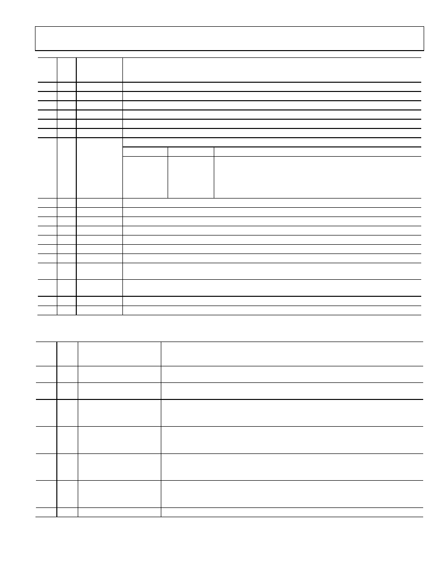
Table 54. LVDS Channel Dividers
Reg.
Addr
(Hex) Bit(s) Name
Description
190
[7:4]
Divider 0 low cycles
Number of clock cycles (minus 1) of the divider input during which divider output stays low.
A value of 0x7 means the divider is low for eight input clock cycles (default: 0x7).
190
[3:0]
Divider 0 high cycles
Number of clock cycles (minus 1) of the divider input during which divider output stays high.
A value of 0x7 means the divider is high for eight input clock cycles (default: 0x7).
191
[7]
Divider 0 bypass
Bypasses and powers down the divider; routes input to divider output.
[7] = 0; use the divider (default).
[7] = 1; bypass the divider.
191
[6]
Divider 0 ignore SYNC
Ignore SYNC.
[6] = 0; obey chip-level SYNC signal (default).
[6] = 1; ignore chip-level SYNC signal.
191
[5]
Divider 0 force high
Forces divider output to high. This requires that ignore SYNC also be set.
[5] = 0; divider output forced to low (default).
[5] = 1; divider output forced to high.
191
[4]
Divider 0 start high
Selects clock output to start high or start low.
[4] = 0; start low (default).
[4] = 1; start high.
191
[3:0]
Divider 0 phase offset
Phase offset (default: 0x0).
相关PDF资料 |
PDF描述 |
|---|---|
| AD9522-1BCPZ-REEL7 | IC CLOCK GEN 2.5GHZ VCO 64LFCSP |
| AD9522-2BCPZ | IC CLOCK GEN 2.2GHZ VCO 64LFCSP |
| AD9522-3BCPZ-REEL7 | IC CLOCK GEN 2GHZ VCO 64LFCSP |
| AD9522-4BCPZ-REEL7 | IC CLOCK GEN 1.6GHZ VCO 64LFCSP |
| AD9522-5BCPZ | IC CLOCK GEN 2.4GHZ 64LFCSP |
相关代理商/技术参数 |
参数描述 |
|---|---|
| AD9522-1 | 制造商:AD 制造商全称:Analog Devices 功能描述:12 LVDS/24 CMOS Output Clock Generator with Integrated 2.4 GHz VCO |
| AD9522-1/PCBZ | 功能描述:BOARD EVAL FOR AD9522-1 CLK GEN RoHS:是 类别:编程器,开发系统 >> 评估演示板和套件 系列:- 标准包装:1 系列:- 主要目的:电信,线路接口单元(LIU) 嵌入式:- 已用 IC / 零件:IDT82V2081 主要属性:T1/J1/E1 LIU 次要属性:- 已供物品:板,电源,线缆,CD 其它名称:82EBV2081 |
| AD9522-1BCPZ | 功能描述:IC CLOCK GEN 2.5GHZ VCO 64LFCSP RoHS:是 类别:集成电路 (IC) >> 时钟/计时 - 时钟发生器,PLL,频率合成器 系列:- 标准包装:1,000 系列:Precision Edge® 类型:时钟/频率合成器 PLL:无 输入:CML,PECL 输出:CML 电路数:1 比率 - 输入:输出:2:1 差分 - 输入:输出:是/是 频率 - 最大:10.7GHz 除法器/乘法器:无/无 电源电压:2.375 V ~ 3.6 V 工作温度:-40°C ~ 85°C 安装类型:表面贴装 封装/外壳:16-VFQFN 裸露焊盘,16-MLF? 供应商设备封装:16-MLF?(3x3) 包装:带卷 (TR) 其它名称:SY58052UMGTRSY58052UMGTR-ND |
| AD9522-1BCPZ-REEL7 | 功能描述:IC CLOCK GEN 2.5GHZ VCO 64LFCSP RoHS:是 类别:集成电路 (IC) >> 时钟/计时 - 时钟发生器,PLL,频率合成器 系列:- 标准包装:2,000 系列:- 类型:PLL 时钟发生器 PLL:带旁路 输入:LVCMOS,LVPECL 输出:LVCMOS 电路数:1 比率 - 输入:输出:2:11 差分 - 输入:输出:是/无 频率 - 最大:240MHz 除法器/乘法器:是/无 电源电压:3.135 V ~ 3.465 V 工作温度:0°C ~ 70°C 安装类型:表面贴装 封装/外壳:32-LQFP 供应商设备封装:32-TQFP(7x7) 包装:带卷 (TR) |
| AD9522-2 | 制造商:AD 制造商全称:Analog Devices 功能描述:12 LVDS/24 CMOS Output Clock Generator with Integrated 2.2 GHz VCO |
发布紧急采购,3分钟左右您将得到回复。