- 您现在的位置:买卖IC网 > PDF目录1987 > AD9522-1BCPZ-REEL7 (Analog Devices Inc)IC CLOCK GEN 2.5GHZ VCO 64LFCSP PDF资料下载
参数资料
| 型号: | AD9522-1BCPZ-REEL7 |
| 厂商: | Analog Devices Inc |
| 文件页数: | 32/84页 |
| 文件大小: | 0K |
| 描述: | IC CLOCK GEN 2.5GHZ VCO 64LFCSP |
| 标准包装: | 750 |
| 类型: | 时钟发生器,扇出配送 |
| PLL: | 是 |
| 输入: | CMOS,LVDS,LVPECL |
| 输出: | CMOS,LVDS |
| 电路数: | 1 |
| 比率 - 输入:输出: | 2:12,2:24 |
| 差分 - 输入:输出: | 是/是 |
| 频率 - 最大: | 2.65GHz |
| 除法器/乘法器: | 是/无 |
| 电源电压: | 3.135 V ~ 3.465 V |
| 工作温度: | -40°C ~ 85°C |
| 安装类型: | 表面贴装 |
| 封装/外壳: | 64-VFQFN 裸露焊盘,CSP |
| 供应商设备封装: | 64-LFCSP-VQ(9x9) |
| 包装: | 带卷 (TR) |
第1页第2页第3页第4页第5页第6页第7页第8页第9页第10页第11页第12页第13页第14页第15页第16页第17页第18页第19页第20页第21页第22页第23页第24页第25页第26页第27页第28页第29页第30页第31页当前第32页第33页第34页第35页第36页第37页第38页第39页第40页第41页第42页第43页第44页第45页第46页第47页第48页第49页第50页第51页第52页第53页第54页第55页第56页第57页第58页第59页第60页第61页第62页第63页第64页第65页第66页第67页第68页第69页第70页第71页第72页第73页第74页第75页第76页第77页第78页第79页第80页第81页第82页第83页第84页
AD9522-1
Rev. 0 | Page 38 of 84
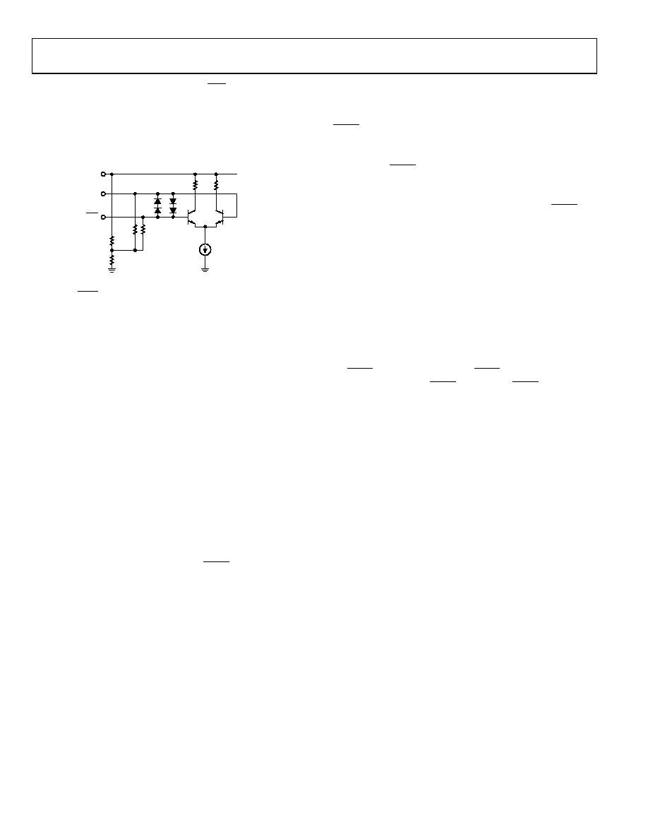
External VCXO/VCO Clock Input (CLK/CLK)
External/Manual Holdover Mode
A manual holdover mode can be enabled that allows the user to
place the charge pump into a high impedance state when the
SYNC pin is asserted low. This operation is edge sensitive, not
level sensitive. The charge pump enters a high impedance state
immediately. To take the charge pump out of a high impedance
state, take the SYNC pin high. The charge pump then leaves the
high impedance state synchronously with the next PFD rising
edge from the reference clock. This prevents extraneous charge
pump events from occurring during the time between SYNC
going high and the next PFD event. This also means that the
charge pump stays in a high impedance state if there is no
reference clock present.
This differential input is used to drive the AD9522 clock
distribution section. This input can receive up to 2.4 GHz.
The pins are internally self-biased, and the input signal should
be ac-coupled via capacitors.
VS
CLOCK INPUT
STAGE
CLK
5k
2.5k
0
722
0-
0
32
The B counter (in the N divider) is reset synchronously with the
charge pump leaving the high impedance state on the reference
path PFD event. This helps align the edges out of the R and N
dividers for faster settling of the PLL. Because the prescaler is
not reset, this feature works best when the B and R numbers are
close because this results in a smaller phase difference for the
loop to settle out.
Figure 46. CLK Equivalent Input Circuit
The CLK/CLK input can be used either as a distribution only
input (with the PLL off), or as a feedback input for an external
VCO/VCXO using the internal PLL when the internal VCO is
not used. These inputs are also used as a feedback path for the
external zero delay mode.
When using this mode, the channel dividers should be set to ignore
the SYNC pin (at least after an initial SYNC event). If the dividers
are not set to ignore the SYNC pin, any time SYNC is taken low
to put the part into holdover, the distribution outputs turn off.
The channel divider ignore SYNC function is found in 0x191[6],
0x194[6], 0x197[6], and 0x19A[6] for Channel Divider 0, Channel
Divider 1, Channel Divider 2, and Channel Divider 3, respectively.
Holdover
The AD9522 PLL has a holdover function. Holdover is
implemented by placing the charge pump in a high impedance
state. This function is useful when the PLL reference clock is
lost. Holdover mode allows the VCO to maintain a relatively
constant frequency even though there is no reference clock.
Without this function, the charge pump is placed into a constant
pump-up or pump-down state, resulting in a massive VCO
frequency shift. Because the charge pump is placed in a high
impedance state, any leakage that occurs at the charge pump
output or the VCO tuning node causes a drift of the VCO
frequency. This can be mitigated by using a loop filter that
contains a large capacitive component because this drift is
limited by the current leakage induced slew rate (ILEAK/C) of
the VCO control voltage.
Automatic/Internal Holdover Mode
When enabled, this function automatically puts the charge
pump into a high impedance state when the loop loses lock.
The assumption is that the only reason the loop loses lock is due
to the PLL losing the reference clock; therefore, the holdover
function puts the charge pump into a high impedance state to
maintain the VCO frequency as close as possible to the original
frequency before the reference clock disappeared.
Both a manual holdover mode, using the SYNC pin, and an
automatic holdover mode are provided. To use either function,
the holdover function must be enabled (0x01D[0]).
A flowchart of the automatic/internal holdover function
operation is shown in Figure 47.
相关PDF资料 |
PDF描述 |
|---|---|
| AD9522-2BCPZ | IC CLOCK GEN 2.2GHZ VCO 64LFCSP |
| AD9522-3BCPZ-REEL7 | IC CLOCK GEN 2GHZ VCO 64LFCSP |
| AD9522-4BCPZ-REEL7 | IC CLOCK GEN 1.6GHZ VCO 64LFCSP |
| AD9522-5BCPZ | IC CLOCK GEN 2.4GHZ 64LFCSP |
| AD9523-1BCPZ-REEL7 | IC INTEGER-N CLCK GEN 72LFCSP |
相关代理商/技术参数 |
参数描述 |
|---|---|
| AD9522-2 | 制造商:AD 制造商全称:Analog Devices 功能描述:12 LVDS/24 CMOS Output Clock Generator with Integrated 2.2 GHz VCO |
| AD9522-2/PCBZ | 功能描述:BOARD EVAL FOR AD9522-2 CLK GEN RoHS:是 类别:编程器,开发系统 >> 评估演示板和套件 系列:- 标准包装:1 系列:- 主要目的:电信,线路接口单元(LIU) 嵌入式:- 已用 IC / 零件:IDT82V2081 主要属性:T1/J1/E1 LIU 次要属性:- 已供物品:板,电源,线缆,CD 其它名称:82EBV2081 |
| AD9522-2BCPZ | 功能描述:IC CLOCK GEN 2.2GHZ VCO 64LFCSP RoHS:是 类别:集成电路 (IC) >> 时钟/计时 - 时钟发生器,PLL,频率合成器 系列:- 标准包装:2,000 系列:- 类型:PLL 时钟发生器 PLL:带旁路 输入:LVCMOS,LVPECL 输出:LVCMOS 电路数:1 比率 - 输入:输出:2:11 差分 - 输入:输出:是/无 频率 - 最大:240MHz 除法器/乘法器:是/无 电源电压:3.135 V ~ 3.465 V 工作温度:0°C ~ 70°C 安装类型:表面贴装 封装/外壳:32-LQFP 供应商设备封装:32-TQFP(7x7) 包装:带卷 (TR) |
| AD9522-2BCPZ-REEL7 | 功能描述:IC CLOCK GEN 2.2GHZ VCO 64LFCSP RoHS:是 类别:集成电路 (IC) >> 时钟/计时 - 时钟发生器,PLL,频率合成器 系列:- 标准包装:2,000 系列:- 类型:PLL 时钟发生器 PLL:带旁路 输入:LVCMOS,LVPECL 输出:LVCMOS 电路数:1 比率 - 输入:输出:2:11 差分 - 输入:输出:是/无 频率 - 最大:240MHz 除法器/乘法器:是/无 电源电压:3.135 V ~ 3.465 V 工作温度:0°C ~ 70°C 安装类型:表面贴装 封装/外壳:32-LQFP 供应商设备封装:32-TQFP(7x7) 包装:带卷 (TR) |
| AD9522-3 | 制造商:AD 制造商全称:Analog Devices 功能描述:12 LVDS/24 CMOS Output Clock Generator with Integrated 2 GHz VCO |
发布紧急采购,3分钟左右您将得到回复。