- 您现在的位置:买卖IC网 > PDF目录1987 > AD9522-1BCPZ-REEL7 (Analog Devices Inc)IC CLOCK GEN 2.5GHZ VCO 64LFCSP PDF资料下载
参数资料
| 型号: | AD9522-1BCPZ-REEL7 |
| 厂商: | Analog Devices Inc |
| 文件页数: | 37/84页 |
| 文件大小: | 0K |
| 描述: | IC CLOCK GEN 2.5GHZ VCO 64LFCSP |
| 标准包装: | 750 |
| 类型: | 时钟发生器,扇出配送 |
| PLL: | 是 |
| 输入: | CMOS,LVDS,LVPECL |
| 输出: | CMOS,LVDS |
| 电路数: | 1 |
| 比率 - 输入:输出: | 2:12,2:24 |
| 差分 - 输入:输出: | 是/是 |
| 频率 - 最大: | 2.65GHz |
| 除法器/乘法器: | 是/无 |
| 电源电压: | 3.135 V ~ 3.465 V |
| 工作温度: | -40°C ~ 85°C |
| 安装类型: | 表面贴装 |
| 封装/外壳: | 64-VFQFN 裸露焊盘,CSP |
| 供应商设备封装: | 64-LFCSP-VQ(9x9) |
| 包装: | 带卷 (TR) |
第1页第2页第3页第4页第5页第6页第7页第8页第9页第10页第11页第12页第13页第14页第15页第16页第17页第18页第19页第20页第21页第22页第23页第24页第25页第26页第27页第28页第29页第30页第31页第32页第33页第34页第35页第36页当前第37页第38页第39页第40页第41页第42页第43页第44页第45页第46页第47页第48页第49页第50页第51页第52页第53页第54页第55页第56页第57页第58页第59页第60页第61页第62页第63页第64页第65页第66页第67页第68页第69页第70页第71页第72页第73页第74页第75页第76页第77页第78页第79页第80页第81页第82页第83页第84页
AD9522-1
Rev. 0 | Page 42 of 84
DIVIDE BY 1,
2, 3, 4, 5, OR 6
LF
CLK/CLK
R
DIVIDER
R
DELAY
N
DIVIDER
N
DELAY
PFD
CP
LOOP
FILTER
MUX1
REG 0x01E[1] = 1
0
1
REFIN/
REFIN
MU
X
3
REG 0x01E[2]
ZERO DELAY
INTERNAL FEEDBACK PATH
EXTERNAL FEEDBACK PATH
ZERO DELAY FEEDBACK CLOCK
CHANNEL DIVIDER 0
CHANNEL DIVIDER 1
CHANNEL DIVIDER 2
CHANNEL DIVIDER 3
OUT0 TO OUT2
OUT3 TO OUT5
OUT6 TO OUT8
OUT9 TO OUT11
AD9522
0
72
20
-05
3
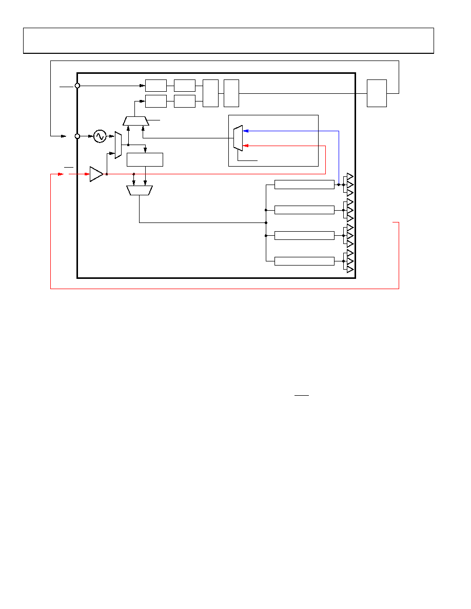
Figure 49. Zero Delay Function
ZERO DELAY OPERATION
Zero delay operation aligns the phase of the output clocks with
the phase of the external PLL reference input. There are two
zero delay modes on the AD9522: internal and external.
Internal Zero Delay Mode
The internal zero delay function of the AD9522 is achieved by
feeding the output of Channel Divider 0 back to the PLL N
divider. In Figure 49, the change in signal routing for internal
zero delay mode is shown in blue.
Set Register 0x01E[2:1] = 01b to select thr internal zero delay
mode. In the internal zero delay mode, the output of Channel
Divider 0 is routed back to the PLL (N divider) through MUX3
and MUX1 (feedback path shown in blue in Figure 49). The PLL
synchronizes the phase/edge of the output of Channel Divider 0
with the phase/edge of the reference input.
Because the channel dividers are synchronized to each other,
the outputs of the channel dividers are synchronous with the
reference input. Both the R delay and the N delay inside the
PLL can be programmed to compensate for the propagation
delay from the output drivers and PLL components to minimize
the phase offset between the clock output and the reference
input to achieve zero delay.
External Zero Delay Mode
The external zero delay function of the AD9522 is achieved by
feeding one clock output back to the CLK input and ultimately
back to the PLL N divider. In Figure 49, the change in signal
routing for external zero delay mode is shown in red.
Set 0x01E[2:1] = 11b to select the external zero delay mode.
In external zero delay mode, one of the twelve output clocks
(OUT0 to OUT11) can be routed back to the PLL (N divider)
through the CLK/CLK pins and through MUX3 and MUX1.
This feedback path is shown in red in
.
The user must specify which channel divider will be used for
external zero delay mode in order for VCO calibration to work
correctly. Channel Divider 0 is the default. Channel Divider 1,
Channel Divider 2, or Channel Divider 3 can be selected for zero
delay feedback by changing the value in Register 0x01E[4:3].
The PLL synchronizes the phase/edge of the feedback output clock
with the phase/edge of the reference input. Because the channel
dividers are synchronized to each other, the clock outputs are
synchronous with the reference input. Both the R delay and the
N delay inside the PLL can be programmed to compensate for
the propagation delay from the PLL components to minimize the
phase offset between the feedback clock and the reference input.
相关PDF资料 |
PDF描述 |
|---|---|
| AD9522-2BCPZ | IC CLOCK GEN 2.2GHZ VCO 64LFCSP |
| AD9522-3BCPZ-REEL7 | IC CLOCK GEN 2GHZ VCO 64LFCSP |
| AD9522-4BCPZ-REEL7 | IC CLOCK GEN 1.6GHZ VCO 64LFCSP |
| AD9522-5BCPZ | IC CLOCK GEN 2.4GHZ 64LFCSP |
| AD9523-1BCPZ-REEL7 | IC INTEGER-N CLCK GEN 72LFCSP |
相关代理商/技术参数 |
参数描述 |
|---|---|
| AD9522-2 | 制造商:AD 制造商全称:Analog Devices 功能描述:12 LVDS/24 CMOS Output Clock Generator with Integrated 2.2 GHz VCO |
| AD9522-2/PCBZ | 功能描述:BOARD EVAL FOR AD9522-2 CLK GEN RoHS:是 类别:编程器,开发系统 >> 评估演示板和套件 系列:- 标准包装:1 系列:- 主要目的:电信,线路接口单元(LIU) 嵌入式:- 已用 IC / 零件:IDT82V2081 主要属性:T1/J1/E1 LIU 次要属性:- 已供物品:板,电源,线缆,CD 其它名称:82EBV2081 |
| AD9522-2BCPZ | 功能描述:IC CLOCK GEN 2.2GHZ VCO 64LFCSP RoHS:是 类别:集成电路 (IC) >> 时钟/计时 - 时钟发生器,PLL,频率合成器 系列:- 标准包装:2,000 系列:- 类型:PLL 时钟发生器 PLL:带旁路 输入:LVCMOS,LVPECL 输出:LVCMOS 电路数:1 比率 - 输入:输出:2:11 差分 - 输入:输出:是/无 频率 - 最大:240MHz 除法器/乘法器:是/无 电源电压:3.135 V ~ 3.465 V 工作温度:0°C ~ 70°C 安装类型:表面贴装 封装/外壳:32-LQFP 供应商设备封装:32-TQFP(7x7) 包装:带卷 (TR) |
| AD9522-2BCPZ-REEL7 | 功能描述:IC CLOCK GEN 2.2GHZ VCO 64LFCSP RoHS:是 类别:集成电路 (IC) >> 时钟/计时 - 时钟发生器,PLL,频率合成器 系列:- 标准包装:2,000 系列:- 类型:PLL 时钟发生器 PLL:带旁路 输入:LVCMOS,LVPECL 输出:LVCMOS 电路数:1 比率 - 输入:输出:2:11 差分 - 输入:输出:是/无 频率 - 最大:240MHz 除法器/乘法器:是/无 电源电压:3.135 V ~ 3.465 V 工作温度:0°C ~ 70°C 安装类型:表面贴装 封装/外壳:32-LQFP 供应商设备封装:32-TQFP(7x7) 包装:带卷 (TR) |
| AD9522-3 | 制造商:AD 制造商全称:Analog Devices 功能描述:12 LVDS/24 CMOS Output Clock Generator with Integrated 2 GHz VCO |
发布紧急采购,3分钟左右您将得到回复。