参数资料
| 型号: | AD9524BCPZ |
| 厂商: | Analog Devices Inc |
| 文件页数: | 14/56页 |
| 文件大小: | 0K |
| 描述: | IC INTEGER-N CLCK GEN 48LFCSP |
| 标准包装: | 1 |
| 类型: | 时钟/频率发生器,扇出缓冲器(分配) |
| PLL: | 是 |
| 主要目的: | 以太网,光纤通道,SONET/SDH |
| 输入: | CMOS |
| 输出: | HSTL,LVCMOS,LVDS,LVPECL |
| 电路数: | 1 |
| 比率 - 输入:输出: | 2:6 |
| 差分 - 输入:输出: | 是/是 |
| 频率 - 最大: | 1GHz |
| 电源电压: | 1.71 V ~ 3.465 V |
| 工作温度: | -40°C ~ 85°C |
| 安装类型: | 表面贴装 |
| 封装/外壳: | 48-VFQFN 裸露焊盘,CSP |
| 供应商设备封装: | 48-LFCSP-VQ(7x7) |
| 包装: | 托盘 |
| 相关产品: | AD9524BCPZ-REEL7DKR-ND - IC INTEGER-N CLCK GEN 48LFCSP AD9524BCPZ-REEL7CT-ND - IC INTEGER-N CLCK GEN 48LFCSP AD9524/PCBZ-ND - BOARD EVAL FOR AD9524 AD9524BCPZ-REEL7TR-ND - IC INTEGER-N CLCK GEN 48LFCSP |
第1页第2页第3页第4页第5页第6页第7页第8页第9页第10页第11页第12页第13页当前第14页第15页第16页第17页第18页第19页第20页第21页第22页第23页第24页第25页第26页第27页第28页第29页第30页第31页第32页第33页第34页第35页第36页第37页第38页第39页第40页第41页第42页第43页第44页第45页第46页第47页第48页第49页第50页第51页第52页第53页第54页第55页第56页
Data Sheet
AD9524
Rev. E | Page 21 of 56
PLL1 Input Dividers
Each reference input feeds a dedicated reference divider block.
The input dividers provide division of the reference frequency
in integer steps from 1 to 1023. They provide the bulk of the
frequency prescaling that is necessary to reduce the reference
frequency to accommodate the bandwidth that is typically
desired for PLL1.
PLL1 Reference Switchover
The reference monitor verifies the presence/absence of the
prescaled REFA and REFB signals (that is, after division by the
input dividers). The status of the reference monitor guides the
activity of the switchover control logic. The AD9524 supports
automatic and manual PLL reference clock switching between
REFA (the REFA and REFA pins) and REFB (the REFB and
REFB pins). This feature supports networking and infrastructure
applications that require redundant references.
There are several configurable modes of reference switchover.
The manual switchover is achieved either via a programming
register setting or by using the REF_SEL pin. The automatic
switchover occurs when REFA disappears and there is a reference
on REFB.
The reference automatic switchover can be set to work as follows:
Nonrevertive: stay on REFB. Switch from REFA to REFB
when REFA disappears, but do not switch back to REFA
if it reappears. If REFB disappears, then go back to REFA.
Revert to REFA. Switch from REFA to REFB when REFA
disappears. Return to REFA from REFB when REFA returns.
See Table 43 for the PLL1 miscellaneous control register bit
settings.
PLL1 Holdover
In the absence of both input references, the device enters holdover
mode. Holdover is a secondary function that is provided by PLL1.
Because PLL1 has an external VCXO available as a frequency
source, it continues to operate in the absence of the input reference
signals. When the device switches to holdover, the charge pump
tristates. The device continues operating in this mode until a
reference signal becomes available. Then the device exits holdover
mode, and PLL1 resynchronizes with the active reference. In
addition to tristate, the charge pump can be forced to VCC/2
during holdover (see Table 43, Bit 6 in Register 0x01C).
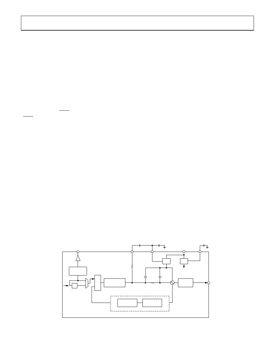
COMPONENT BLOCKS—OUTPUT PLL (PLL2)
PLL2 General Description
The output PLL (referred to as PLL2) consists of an optional input
reference doubler, phase-frequency detector (PFD), a partially
integrated analog loop filter (see Figure 25), an integrated
voltage-controlled oscillator (VCO), and a feedback divider.
The VCO produces a nominal 3.8 GHz signal with an output
divider that is capable of division ratios of 4 to 11.
The PFD of the output PLL drives a charge pump that increases,
decreases, or holds constant the charge stored on the loop filter
capacitors (both internal and external). The stored charge results
in a voltage that sets the output frequency of the VCO. The
feedback loop of the PLL causes the VCO control voltage to
vary in a way that phase locks the PFD input signals.
The gain of PLL2 is proportional to the current delivered by the
charge pump. The loop filter bandwidth is chosen to reduce noise
contributions from PLL sources that could degrade phase noise
requirements.
The output PLL has a VCO with multiple bands spanning a
range of 3.6 GHz to 4.0 GHz. However, the actual operating
frequency within a particular band depends on the control
voltage that appears on the loop filter capacitor. The control
voltage causes the VCO output frequency to vary linearly within
the selected band. This frequency variability allows the control
loop of the output PLL to synchronize the VCO output signal
with the reference signal applied to the PFD. Typically, the
device automatically selects the appropriate band as part of its
calibration process (invoked via the VCO control register at
Address 0x0F3).
N DIVIDER
TO DIST/
RESYNC
×2
PLL1_OUT
LDO
PLL_1.8V
LDO_PLL2
VDD3_PLL2
LDO_VCO
DIVIDE BY
1, 2, 4, 8, 16
DIVIDE BY
4, 5, 6, ...11
DIVIDE-BY-4
PRESCALER
A/B
COUNTERS
CHARGE PUMP
8 BITS, 3.5A LSB
PFD
RZERO
RPOLE2
CPOLE1
CPOLE2
LF2_EXT_CAP
AD9524
09081
-023
Figure 25. Output PLL (PLL2) Block Diagram
相关PDF资料 |
PDF描述 |
|---|---|
| AD9540BCPZ-REEL7 | IC CLOCK GEN/SYNTHESIZER 48LFCSP |
| AD9547BCPZ-REEL7 | IC CLOCK GEN/SYNCHRONIZR 64LFCSP |
| AD9548BCPZ-REEL7 | IC CLOCK GEN/SYNCHRONIZR 88LFCSP |
| AD9549ABCPZ-REEL7 | IC CLOCK GEN/SYNCHRONIZR 64LFCSP |
| AD9550BCPZ-REEL7 | IC INTEGER-N TRANSLATOR 32-LFCSP |
相关代理商/技术参数 |
参数描述 |
|---|---|
| AD9524BCPZ-REEL7 | 功能描述:IC INTEGER-N CLCK GEN 48LFCSP RoHS:是 类别:集成电路 (IC) >> 时钟/计时 - 专用 系列:- 标准包装:28 系列:- 类型:时钟/频率发生器 PLL:是 主要目的:Intel CPU 服务器 输入:时钟 输出:LVCMOS 电路数:1 比率 - 输入:输出:3:22 差分 - 输入:输出:无/是 频率 - 最大:400MHz 电源电压:3.135 V ~ 3.465 V 工作温度:0°C ~ 85°C 安装类型:表面贴装 封装/外壳:64-TFSOP (0.240",6.10mm 宽) 供应商设备封装:64-TSSOP 包装:管件 |
| AD9525 | 制造商:AD 制造商全称:Analog Devices 功能描述:Low Jitter Clock Generator with Eight LVPECL Outputs |
| AD9525/PCBZ | 功能描述:时钟和定时器开发工具 Evaluation kit 2950MHz VCO installed RoHS:否 制造商:Texas Instruments 产品:Evaluation Modules 类型:Clock Conditioners 工具用于评估:LMK04100B 频率:122.8 MHz 工作电源电压:3.3 V |
| AD9525/PCBZ-VCO | 功能描述:时钟和定时器开发工具 Evaluation kit CRO29508 VCO installed RoHS:否 制造商:Texas Instruments 产品:Evaluation Modules 类型:Clock Conditioners 工具用于评估:LMK04100B 频率:122.8 MHz 工作电源电压:3.3 V |
| AD9525BCPZ | 功能描述:时钟发生器及支持产品 High performance clock distributor Exter RoHS:否 制造商:Silicon Labs 类型:Clock Generators 最大输入频率:14.318 MHz 最大输出频率:166 MHz 输出端数量:16 占空比 - 最大:55 % 工作电源电压:3.3 V 工作电源电流:1 mA 最大工作温度:+ 85 C 安装风格:SMD/SMT 封装 / 箱体:QFN-56 |
发布紧急采购,3分钟左右您将得到回复。