- 您现在的位置:买卖IC网 > PDF目录1987 > AD9549ABCPZ-REEL7 (Analog Devices Inc)IC CLOCK GEN/SYNCHRONIZR 64LFCSP PDF资料下载
参数资料
| 型号: | AD9549ABCPZ-REEL7 |
| 厂商: | Analog Devices Inc |
| 文件页数: | 1/76页 |
| 文件大小: | 0K |
| 描述: | IC CLOCK GEN/SYNCHRONIZR 64LFCSP |
| 产品变化通告: | AD9549A Mask Change 22/Oct/2010 |
| 标准包装: | 750 |
| 类型: | 时钟/频率发生器,同步器 |
| PLL: | 是 |
| 主要目的: | 以太网,SONET/SDH,Stratum |
| 输入: | CMOS,LVDS,LVPECL |
| 输出: | CMOS,HSTL |
| 电路数: | 1 |
| 比率 - 输入:输出: | 2:2 |
| 差分 - 输入:输出: | 是/是 |
| 频率 - 最大: | 750MHz |
| 电源电压: | 1.71 V ~ 3.465 V |
| 工作温度: | -40°C ~ 85°C |
| 安装类型: | 表面贴装 |
| 封装/外壳: | 64-VFQFN 裸露焊盘,CSP |
| 供应商设备封装: | 64-LFCSP-VQ(9x9) |
| 包装: | 带卷 (TR) |
当前第1页第2页第3页第4页第5页第6页第7页第8页第9页第10页第11页第12页第13页第14页第15页第16页第17页第18页第19页第20页第21页第22页第23页第24页第25页第26页第27页第28页第29页第30页第31页第32页第33页第34页第35页第36页第37页第38页第39页第40页第41页第42页第43页第44页第45页第46页第47页第48页第49页第50页第51页第52页第53页第54页第55页第56页第57页第58页第59页第60页第61页第62页第63页第64页第65页第66页第67页第68页第69页第70页第71页第72页第73页第74页第75页第76页
Dual Input Network Clock
Generator/Synchronizer
AD9549
Rev. D
Information furnished by Analog Devices is believed to be accurate and reliable. However, no
responsibilityisassumedbyAnalogDevicesforitsuse,norforanyinfringementsofpatentsorother
rightsofthirdpartiesthatmayresultfromitsuse.Specificationssubjecttochangewithoutnotice.No
license is granted by implication or otherwise under any patent or patent rights of Analog Devices.
Trademarksandregisteredtrademarksarethepropertyoftheirrespectiveowners.
One Technology Way, P.O. Box 9106, Norwood, MA 02062-9106, U.S.A.
Tel: 781.329.4700
Fax: 781.461.3113
2007–2010 Analog Devices, Inc. All rights reserved.
FEATURES
Flexible reference inputs
Input frequencies: 8 kHz to 750 MHz
Two reference inputs
Loss of reference indicators
Auto and manual holdover modes
Auto and manual switchover modes
Smooth A-to-B phase transition on outputs
Excellent stability in holdover mode
Programmable 16 + 1-bit input divider, R
Differential HSTL clock output
Output frequencies to 750 MHz
Low jitter clock doubler for frequencies of >400 MHz
Single-ended CMOS output for frequencies of <150 MHz
Programmable digital loop filter (<1 Hz to ~100 kHz)
High speed digitally controlled oscillator (DCO) core
Direct digital synthesizer (DDS) with integrated 14-bit DAC
Excellent dynamic performance
Programmable 16 + 1-bit feedback divider, S
Software controlled power-down
Available 64-lead LFCSP package
APPLICATIONS
Network synchronization
Reference clock jitter cleanup
SONET/SDH clocks up to OC-192, including FEC
Stratum 3/3E reference clocks
Wireless base station, controllers
Cable infrastructure
Data communications
GENERAL DESCRIPTION
The AD9549 provides synchronization for many systems,
including synchronous optical networks (SONET/SDH). The
AD9549 generates an output clock, synchronized to one of two
external input references. The external references may contain
significant time jitter, also specified as phase noise. Using a
digitally controlled loop and holdover circuitry, the AD9549
continues to generate a clean (low jitter), valid output clock during
a loss of reference condition, even when both references have failed.
The AD9549 operates over an industrial temperature range of
40°C to +85°C.
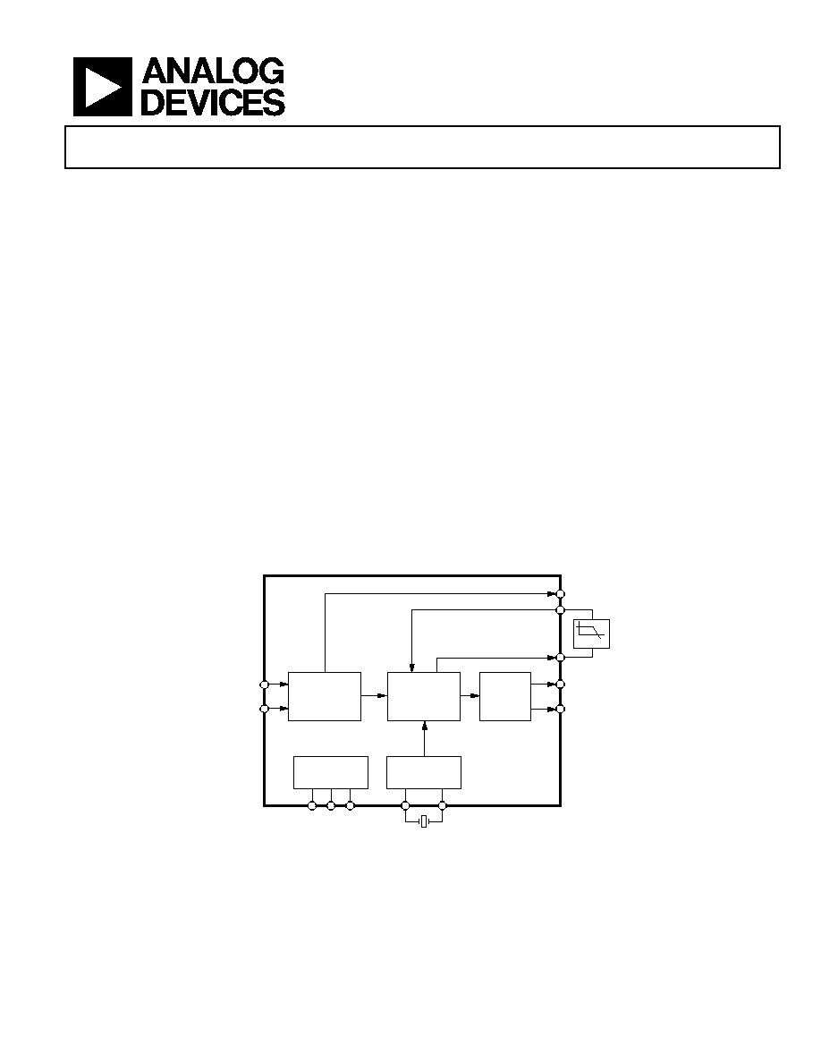
BASIC BLOCK DIAGRAM
FDBK_IN
DAC_OUT
AD9549
REFA_IN
REFB_IN
S1 TO S4
OUT
OUT_CMOS
R
DIGITAL INTERFACE
FILTER
SYSTEM CLOCK
MULTIPLIER
SERIAL PORT,
I/O LOGIC
REFERENCE
MONITORS
AND
SWITCHING
DIGITAL PLL
R, S DIVIDERS
HOLDOVER
CLOCK
OUTPUT
DRIVERS
06744-
001
Figure 1.
相关PDF资料 |
PDF描述 |
|---|---|
| AD9550BCPZ-REEL7 | IC INTEGER-N TRANSLATOR 32-LFCSP |
| AD9551BCPZ | IC CLOCK GEN MULTISERV 40-LFCSP |
| AD9552BCPZ-REEL7 | IC PLL CLOCK GEN LP 32LFCSP |
| AD9553BCPZ-REEL7 | IC INTEGER-N CLCK GEN 32LFCSP |
| AD9557BCPZ-REEL7 | IC CLK XLATR PLL 1250MHZ 40LFCSP |
相关代理商/技术参数 |
参数描述 |
|---|---|
| AD9549APCBZ | 制造商:AD 制造商全称:Analog Devices 功能描述:Dual Input Network Clock Generator/Synchronizer |
| AD9549BCPZ | 制造商:Analog Devices 功能描述: |
| AD9549BCPZ-REEL7 | 制造商:Analog Devices 功能描述:PLL CLOCK SYNTHESIZER SGL 64LFCSP EP - Tape and Reel |
| AD9549BCPZ-TR | 制造商:Analog Devices 功能描述:650MHZ DDS CLK GEN W/SYNCH REEL - Tape and Reel |
| AD9549XCPZ | 制造商:AD 制造商全称:Analog Devices 功能描述:Dual Input Network Clock Generator/Synchronizer |
发布紧急采购,3分钟左右您将得到回复。