- 您现在的位置:买卖IC网 > PDF目录1987 > AD9549ABCPZ-REEL7 (Analog Devices Inc)IC CLOCK GEN/SYNCHRONIZR 64LFCSP PDF资料下载
参数资料
| 型号: | AD9549ABCPZ-REEL7 |
| 厂商: | Analog Devices Inc |
| 文件页数: | 27/76页 |
| 文件大小: | 0K |
| 描述: | IC CLOCK GEN/SYNCHRONIZR 64LFCSP |
| 产品变化通告: | AD9549A Mask Change 22/Oct/2010 |
| 标准包装: | 750 |
| 类型: | 时钟/频率发生器,同步器 |
| PLL: | 是 |
| 主要目的: | 以太网,SONET/SDH,Stratum |
| 输入: | CMOS,LVDS,LVPECL |
| 输出: | CMOS,HSTL |
| 电路数: | 1 |
| 比率 - 输入:输出: | 2:2 |
| 差分 - 输入:输出: | 是/是 |
| 频率 - 最大: | 750MHz |
| 电源电压: | 1.71 V ~ 3.465 V |
| 工作温度: | -40°C ~ 85°C |
| 安装类型: | 表面贴装 |
| 封装/外壳: | 64-VFQFN 裸露焊盘,CSP |
| 供应商设备封装: | 64-LFCSP-VQ(9x9) |
| 包装: | 带卷 (TR) |
第1页第2页第3页第4页第5页第6页第7页第8页第9页第10页第11页第12页第13页第14页第15页第16页第17页第18页第19页第20页第21页第22页第23页第24页第25页第26页当前第27页第28页第29页第30页第31页第32页第33页第34页第35页第36页第37页第38页第39页第40页第41页第42页第43页第44页第45页第46页第47页第48页第49页第50页第51页第52页第53页第54页第55页第56页第57页第58页第59页第60页第61页第62页第63页第64页第65页第66页第67页第68页第69页第70页第71页第72页第73页第74页第75页第76页
AD9549
Rev. D | Page 33 of 76
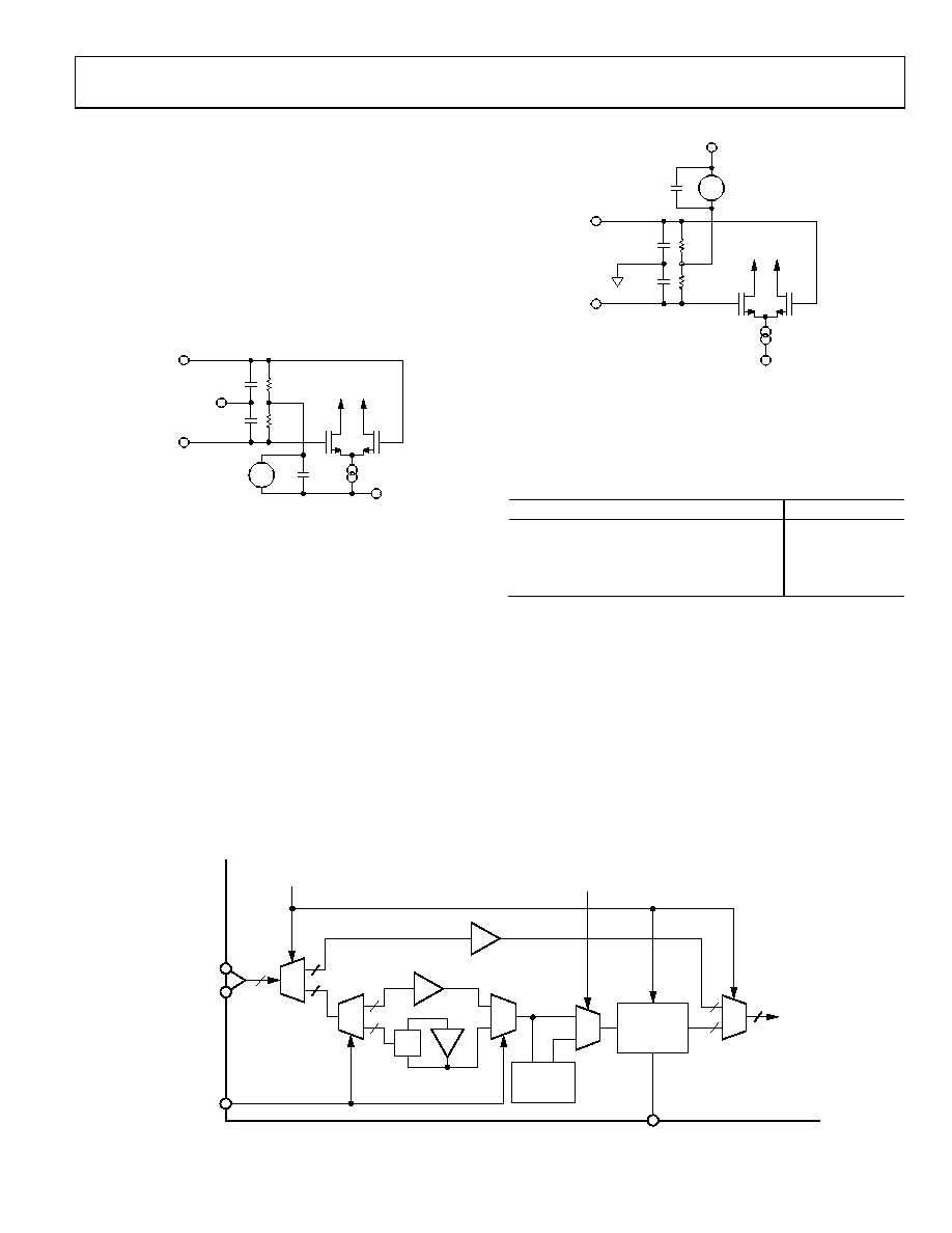
FDBK_IN INPUTS
The feedback pins, FDBK_IN and FDBK_INB, serve as the input
to the feedback path of the digital PLL. Typically, these pins are
used to receive the signal generated by the DDS after it has been
band-limited by the external reconstruction filter.
A diagram of the FDBK input pins is provided in Figure 40,
which includes some of the internal components used to bias
the input circuitry. Note that the FDBK input pins are internally
biased to a dc level of ~1 V. Care should be taken to ensure that
any external connections do not disturb the dc bias because this
may significantly degrade performance.
06744-
040
15k
15k
~1pF
TO S-DIVIDER
AND CLOCK
OUTPUT SECTION
VSS
~1V
VSS
~2pF
+
FDBK_IN
FDBK_INB
Figure 40. Differential FDBK Inputs
REFERENCE INPUTS
Reference Clock Receiver
The reference clock receiver is the point at which the user
supplies the input clock signal that the synchronizer synthesizes
into an output clock. The clock receiver circuit is able to handle
a relatively broad range of input levels as well as frequencies
from 8 kHz up to 750 MHz.
Figure 41 is a diagram of the REFA and REFB input pins, which
includes some of the internal components used to bias the input
circuitry. Note that the REF input pins are internally biased by a
dc source, VB. Care should be taken to ensure that any external
connections do not disturb the dc bias because such a disturbance
may significantly degrade performance.
Note that support for redundant reference clocks is achieved by
using the two reference clock receivers (REFA and REFB).
06744-
041
8k
8k
~1pF
TO REFERENCE
MONITOR AND
SWITCHING LOGIC
VB
VSS
+
REFA_IN
(OR REFB_IN)
REFA_INB
(OR REFB_INB)
VDD
1pF
GND
Figure 41. Reference Inputs
To accommodate a variety of input signal conditions, the value
of VB is programmable via a pair of bits in the I/O register map.
Table 6. Setting of Input Bias Voltage (VB)
Reference Bias Level, Register 0x040F[1:0]
V
B
00 (default)
AVDD3 800 mV
01
AVDD3 400 mV
10
AVDD3 1600 mV
11
AVDD3 1200 mV
SYSCLK INPUTS
Functional Description
The SYSCLK pins are where an external time base is connected
to the AD9549 for generating the internal high frequency
system clock (fS).
The SYSCLK inputs can be operated in one of three modes:
SYSCLK PLL bypassed
SYSCLK PLL enabled with input signal generated externally
Crystal resonator with SYSCLK PLL enabled
A functional diagram of the system clock generator is shown in
06744-
042
1
0
1
0
1
0
BIPOLAR
EDGE
DETECTOR
2
WITH CRYSTAL
RESONATOR
2
1
0
2
SYSCLK
PLL
ENABLED
WITH EXTERNAL DRIVE
SYSCLK PLL BYPASSED
SYSCLK
PLL
MULTIPLIER
1
0
2× REFERENCE FREQUENCY DOUBLER
(I/O REGISTER BIT)
PD SYSCLK PLL
(I/O REGISTER BIT)
DAC
SAMPLE
CLOCK
LOOP_FILTER
SYSCLK
SYSCLKB
CLKMODESEL
2
Figure 42. System Clock Generator Block Diagram
相关PDF资料 |
PDF描述 |
|---|---|
| AD9550BCPZ-REEL7 | IC INTEGER-N TRANSLATOR 32-LFCSP |
| AD9551BCPZ | IC CLOCK GEN MULTISERV 40-LFCSP |
| AD9552BCPZ-REEL7 | IC PLL CLOCK GEN LP 32LFCSP |
| AD9553BCPZ-REEL7 | IC INTEGER-N CLCK GEN 32LFCSP |
| AD9557BCPZ-REEL7 | IC CLK XLATR PLL 1250MHZ 40LFCSP |
相关代理商/技术参数 |
参数描述 |
|---|---|
| AD9549APCBZ | 制造商:AD 制造商全称:Analog Devices 功能描述:Dual Input Network Clock Generator/Synchronizer |
| AD9549BCPZ | 制造商:Analog Devices 功能描述: |
| AD9549BCPZ-REEL7 | 制造商:Analog Devices 功能描述:PLL CLOCK SYNTHESIZER SGL 64LFCSP EP - Tape and Reel |
| AD9549BCPZ-TR | 制造商:Analog Devices 功能描述:650MHZ DDS CLK GEN W/SYNCH REEL - Tape and Reel |
| AD9549XCPZ | 制造商:AD 制造商全称:Analog Devices 功能描述:Dual Input Network Clock Generator/Synchronizer |
发布紧急采购,3分钟左右您将得到回复。