- 您现在的位置:买卖IC网 > PDF目录1987 > AD9549ABCPZ-REEL7 (Analog Devices Inc)IC CLOCK GEN/SYNCHRONIZR 64LFCSP PDF资料下载
参数资料
| 型号: | AD9549ABCPZ-REEL7 |
| 厂商: | Analog Devices Inc |
| 文件页数: | 17/76页 |
| 文件大小: | 0K |
| 描述: | IC CLOCK GEN/SYNCHRONIZR 64LFCSP |
| 产品变化通告: | AD9549A Mask Change 22/Oct/2010 |
| 标准包装: | 750 |
| 类型: | 时钟/频率发生器,同步器 |
| PLL: | 是 |
| 主要目的: | 以太网,SONET/SDH,Stratum |
| 输入: | CMOS,LVDS,LVPECL |
| 输出: | CMOS,HSTL |
| 电路数: | 1 |
| 比率 - 输入:输出: | 2:2 |
| 差分 - 输入:输出: | 是/是 |
| 频率 - 最大: | 750MHz |
| 电源电压: | 1.71 V ~ 3.465 V |
| 工作温度: | -40°C ~ 85°C |
| 安装类型: | 表面贴装 |
| 封装/外壳: | 64-VFQFN 裸露焊盘,CSP |
| 供应商设备封装: | 64-LFCSP-VQ(9x9) |
| 包装: | 带卷 (TR) |
第1页第2页第3页第4页第5页第6页第7页第8页第9页第10页第11页第12页第13页第14页第15页第16页当前第17页第18页第19页第20页第21页第22页第23页第24页第25页第26页第27页第28页第29页第30页第31页第32页第33页第34页第35页第36页第37页第38页第39页第40页第41页第42页第43页第44页第45页第46页第47页第48页第49页第50页第51页第52页第53页第54页第55页第56页第57页第58页第59页第60页第61页第62页第63页第64页第65页第66页第67页第68页第69页第70页第71页第72页第73页第74页第75页第76页
AD9549
Rev. D | Page 24 of 76
The resulting loop filter coefficients for the lower loop
bandwidth, along with the necessary programming values,
are shown as follows:
α = 0.005883404361345
α0 = 1542 (0x606)
α1 = 0 (0x00)
α2 = 7 (0x07)
β = 0.000003820176667
β0 = 16 (0x10)
β1 = 7 (0x07)
γ = 0.00000461136116
γ0 = 19 (0x13)
γ1 = 7 (0x07)
The AD9549 evaluation software generates these coefficients
automatically based on the user’s desired loop characteristics.
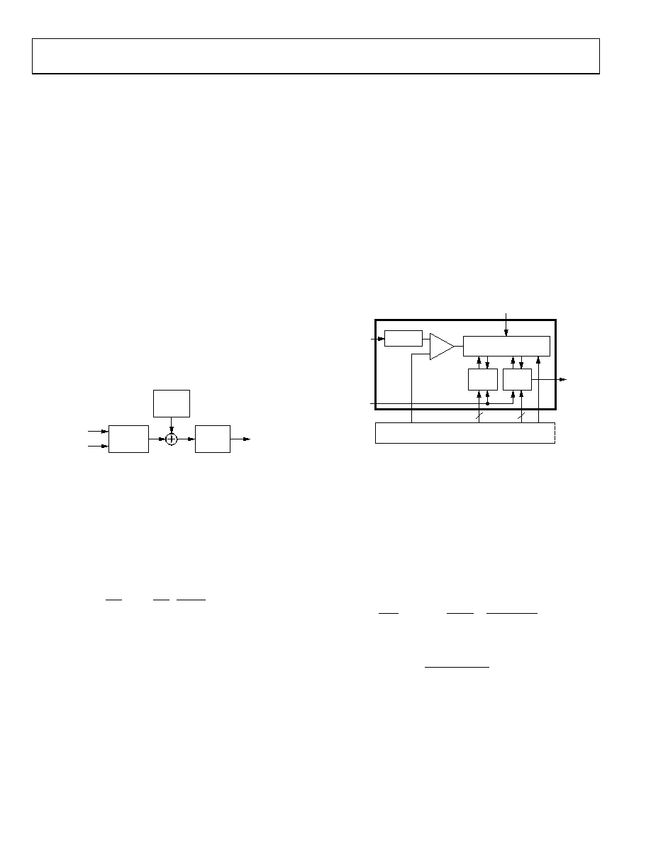
CLOSED-LOOP PHASE OFFSET
The AD9549 provides for limited control over the phase offset
between the reference input signal and the output signal by adding
a constant phase offset value to the output of the phase detector.
An adder is included at the output of the phase detector to support
is set via the DPLL phase offset bits.
06744-
028
PHASE
OFFSET
VALUE
PHASE
DETECTOR
LOOP
FILTER
TO CCI
FILTER
CLK
FEEDBACK
Figure 28. Input Phase Offset Adder
PLLOFFSET is a function of the phase detector gain and the
desired amount of timing offset (ΔtOFFSET). It is given by
PLLOFFSET = ΔtOFFSET(210 × 107 × FPFD_Gain
FPFD_Gain is described in the Fine Phase Detector section.
For example, suppose that FPFD_Gain = 200, fCLK = 3 MHz, and
1° of phase offset is desired. First, the value of ΔtOFFSET must be
determined, as follows:
ps
9
.
925
MHz
3
1
360
1
360
deg
=
=
CLK
OFFSET
t
Having determined ΔtOFFSET,
1896
)
200
10
2
ps(
9
.
925
7
10
=
×
=
OFFSET
PLL
The result has been rounded because PLLOFFSET is restricted to
integer values.
Note that the PLLOFFSET value is programmed as a 14-bit, twos
complement number. However, the user must ensure that the
magnitude is constrained to 12 bits, such that:
211 ≤ PLLOFFSET < +211
The preceding constraint yields a timing adjustment range of
±1 ns. This ensures that the phase offset remains within the
bounds of the fine phase detector.
LOCK DETECTION
Phase Lock Detection
During the phase locking process, the output of the phase
detector tends toward a value of 0, which indicates perfect
alignment of the phase detector input signals. As the control
loop works to maintain the alignment of the phase detector
input signals, the output of the phase detector wanders around 0.
The phase lock detector tracks the absolute value of the digital
samples generated by the phase detector. These samples are
compared to the phase lock detect threshold value (PLDT)
programmed in the I/O register map. A false state at the output
of the comparator indicates that the absolute value of a sample
exceeds the value in the threshold bits. A true state at the output
of the comparator indicates alignment of the phase detector
input signals to the degree specified by the lock detection
threshold.
06744-
029
ABSOLUTE
VALUE
DIGITAL
COMPARATOR
CONTROL LOGIC
UNLOCK
TIMER
LOCK
TIMER
PHASE LOCK DETECT
THRESHOLD
Y
X
CLOSE
LOOP
PHASE
LOCK
DETECT
RESET
P-DIVIDER
CLOCK
PHASE
DETECTOR
SAMPLES
I/O
REGISTERS
3
5
Figure 29. Phase Lock Detector Block Diagram
The phase lock detect threshold value is a 32-bit number stored
in the I/O register map.
(
)
Gain
FPFD
t
PLDT
_
10
2
round
7
10
×
=
where Δt is the maximum allowable timing error between the
signals at the input to the phase detector and the value of
FPFD_Gain is as described in the Fine Phase Detector section.
For example, suppose that fR/R = 3 MHz, FPFD_Gain = 200, and
the maximum timing deviation is given as 1°. This yields a Δt
value of
(
)
10
3
(
360
1
360
1
6
×
=
×
°
=
R
f
R
T
R
t
The resulting phase lock detect threshold is
1896
)
10
3
(
360
200
10
2
round
6
7
10
=
×
=
PLDT
Hence, 1896 (0x00000768) is the value that must be stored in
the phase lock detect threshold bits.
相关PDF资料 |
PDF描述 |
|---|---|
| AD9550BCPZ-REEL7 | IC INTEGER-N TRANSLATOR 32-LFCSP |
| AD9551BCPZ | IC CLOCK GEN MULTISERV 40-LFCSP |
| AD9552BCPZ-REEL7 | IC PLL CLOCK GEN LP 32LFCSP |
| AD9553BCPZ-REEL7 | IC INTEGER-N CLCK GEN 32LFCSP |
| AD9557BCPZ-REEL7 | IC CLK XLATR PLL 1250MHZ 40LFCSP |
相关代理商/技术参数 |
参数描述 |
|---|---|
| AD9549APCBZ | 制造商:AD 制造商全称:Analog Devices 功能描述:Dual Input Network Clock Generator/Synchronizer |
| AD9549BCPZ | 制造商:Analog Devices 功能描述: |
| AD9549BCPZ-REEL7 | 制造商:Analog Devices 功能描述:PLL CLOCK SYNTHESIZER SGL 64LFCSP EP - Tape and Reel |
| AD9549BCPZ-TR | 制造商:Analog Devices 功能描述:650MHZ DDS CLK GEN W/SYNCH REEL - Tape and Reel |
| AD9549XCPZ | 制造商:AD 制造商全称:Analog Devices 功能描述:Dual Input Network Clock Generator/Synchronizer |
发布紧急采购,3分钟左右您将得到回复。