- 您现在的位置:买卖IC网 > PDF目录1987 > AD9549ABCPZ-REEL7 (Analog Devices Inc)IC CLOCK GEN/SYNCHRONIZR 64LFCSP PDF资料下载
参数资料
| 型号: | AD9549ABCPZ-REEL7 |
| 厂商: | Analog Devices Inc |
| 文件页数: | 11/76页 |
| 文件大小: | 0K |
| 描述: | IC CLOCK GEN/SYNCHRONIZR 64LFCSP |
| 产品变化通告: | AD9549A Mask Change 22/Oct/2010 |
| 标准包装: | 750 |
| 类型: | 时钟/频率发生器,同步器 |
| PLL: | 是 |
| 主要目的: | 以太网,SONET/SDH,Stratum |
| 输入: | CMOS,LVDS,LVPECL |
| 输出: | CMOS,HSTL |
| 电路数: | 1 |
| 比率 - 输入:输出: | 2:2 |
| 差分 - 输入:输出: | 是/是 |
| 频率 - 最大: | 750MHz |
| 电源电压: | 1.71 V ~ 3.465 V |
| 工作温度: | -40°C ~ 85°C |
| 安装类型: | 表面贴装 |
| 封装/外壳: | 64-VFQFN 裸露焊盘,CSP |
| 供应商设备封装: | 64-LFCSP-VQ(9x9) |
| 包装: | 带卷 (TR) |
第1页第2页第3页第4页第5页第6页第7页第8页第9页第10页当前第11页第12页第13页第14页第15页第16页第17页第18页第19页第20页第21页第22页第23页第24页第25页第26页第27页第28页第29页第30页第31页第32页第33页第34页第35页第36页第37页第38页第39页第40页第41页第42页第43页第44页第45页第46页第47页第48页第49页第50页第51页第52页第53页第54页第55页第56页第57页第58页第59页第60页第61页第62页第63页第64页第65页第66页第67页第68页第69页第70页第71页第72页第73页第74页第75页第76页
AD9549
Rev. D | Page 19 of 76
The DCO has a minimum frequency, fDCO[MIN] (see the DAC
Output Characteristics section of the AC Specifications table).
This minimum frequency imposes a lower bound, SMIN, on the
feedback divider value, as well.
=
1
,
max
]
[
R
MIN
DCO
MIN
f
R
S
Note that reduced DCO frequencies result in worse jitter
performance (a consequence of the reduced slew rate of the
sinusoid generated by the DDS).
Forward and Reverse FEC Clock Scaling
The feedforward divider (divide-by-R) and feedback divider
(divide-by-S) enable FEC clock scaling. For instance, to multiply
the incoming signal by 255/237, set the S-divider to 255 and the
R-divider to 237. Be careful to abide by the limitations on the R-
and S-dividers, and make sure the phase detector input frequency
is within specified limits.
Phase Detector
The phase detector is composed of two detectors: a coarse phase
detector and a fine phase detector. The two detectors operate in
parallel. Both detectors measure the duration (Δt) of the pulses
generated by a conventional three-state phase/frequency detector.
Together, the fine and coarse phase detectors produce a digital
word that is a time-to-digital conversion of the separation
between the edge transitions of the prescaled reference signal
and the feedback signal.
If the fine phase detector is able to produce a valid result, this
result alone serves as the phase error measurement. If the fine
phase detector is in either an overflow or underflow condition,
the phase error measurement uses the coarse phase detector
instead.
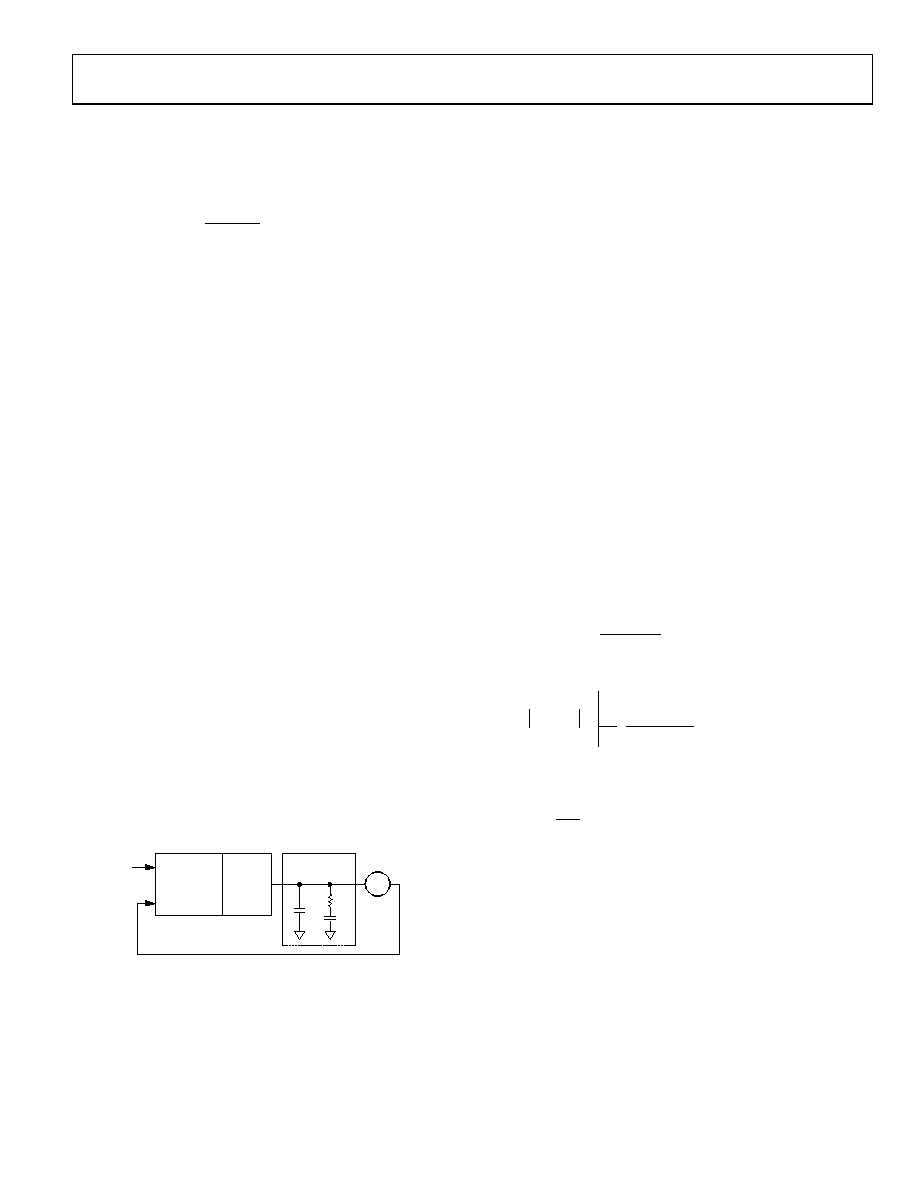
Digital Loop Filter
The digital loop filter integrates and low-pass filters the digital
phase error values delivered by the phase detector. The loop
filter response mimics that of a second-order RC network used
to filter the output of a typical phase detector and charge pump
combination, as shown in Figure 24.
R2
C2
C1
LOOP FILTER
VCO
PHASE/
FREQUENCY
DETECTOR
CHANGE
PUMP
CLK
06744-
024
Figure 24. Typical Analog PLL Block Diagram
The building blocks implemented on the AD9549, however, are
digital. A time-to-digital converter that produces digital values
proportional to the edge timing error between the CLK and
feedback signals replaces the phase-frequency detector and
charge pump. A digital filter that processes the edge timing
error samples from the time-to-digital converter replaces the loop
filter. A DDS replaces the VCO, which produces a frequency that
is linearly related to the digital value provided by the loop filter.
This is shown in Figure 25 with some additional detail.
The samples provided by the time-to-digital converter are delivered
to the loop filter at a sample rate equal to the CLK frequency (that
is, fR/R). The loop filter is intended to oversample the time-to-
digital converter output at a rate determined by the P-divider.
The value of P is programmable via the I/O register map. It is
stored as a 5-bit number, PIO. The value of PIO is related to P by
the equation
P = 2PIO
where 5 ≤ PIO ≤ 16.
Hence, the P-divider can provide divide ratios between 32 and
65,536 in power-of-2 steps. With a DAC sample rate of 1 GHz,
the loop filter sample rate can range from as low as 15.26 kHz to
a maximum of 31.25 MHz. Coupled to the loop filter is a cascaded
comb integrator (CCI) filter that provides a sample rate translation
between the loop filter sample rate (fS/P) and the DDS sample
rate, fS.
The choice of P is important because it controls both the
response of the CCI filter and the sample rate of the loop filter.
To understand the method for determining a useful value for P,
it is first necessary to examine the transfer function of the CCI
filter.
2
P
1
(
1
)
(
=
jω
jω
CCI
e
P
e
ω
H
or
0
,
)
cos(
1
)
cos(
1
0
,1
)
(
2
>
=
ω
ωP
p
ω
HCCI
To evaluate the response in terms of absolute frequency, make
the substitution
S
f
ω
π
= 2
where fS is the DAC sample rate, and f is the frequency at which
HCCI is to be evaluated.
Analysis of this function reveals that the CCI magnitude response
follows a low-pass characteristic that consists of a series of P lobes.
The lobes are bounded by null points occurring at frequency mul-
tiples of fS/P. The peak of each successive lobe is lower than its
predecessor over the frequency range between dc and one-half fS.
For frequencies greater than one-half fS, the response is a reflection
about the vertical at one-half fS. Furthermore, the first lobe (which
appears between dc and fS/P) exhibits a monotonically decreasing
response. That is, the magnitude is unity at dc, and it steadily
decreases with frequency until it vanishes at the first null point
(fS/P).
相关PDF资料 |
PDF描述 |
|---|---|
| AD9550BCPZ-REEL7 | IC INTEGER-N TRANSLATOR 32-LFCSP |
| AD9551BCPZ | IC CLOCK GEN MULTISERV 40-LFCSP |
| AD9552BCPZ-REEL7 | IC PLL CLOCK GEN LP 32LFCSP |
| AD9553BCPZ-REEL7 | IC INTEGER-N CLCK GEN 32LFCSP |
| AD9557BCPZ-REEL7 | IC CLK XLATR PLL 1250MHZ 40LFCSP |
相关代理商/技术参数 |
参数描述 |
|---|---|
| AD9549APCBZ | 制造商:AD 制造商全称:Analog Devices 功能描述:Dual Input Network Clock Generator/Synchronizer |
| AD9549BCPZ | 制造商:Analog Devices 功能描述: |
| AD9549BCPZ-REEL7 | 制造商:Analog Devices 功能描述:PLL CLOCK SYNTHESIZER SGL 64LFCSP EP - Tape and Reel |
| AD9549BCPZ-TR | 制造商:Analog Devices 功能描述:650MHZ DDS CLK GEN W/SYNCH REEL - Tape and Reel |
| AD9549XCPZ | 制造商:AD 制造商全称:Analog Devices 功能描述:Dual Input Network Clock Generator/Synchronizer |
发布紧急采购,3分钟左右您将得到回复。