参数资料
| 型号: | AD9524BCPZ |
| 厂商: | Analog Devices Inc |
| 文件页数: | 18/56页 |
| 文件大小: | 0K |
| 描述: | IC INTEGER-N CLCK GEN 48LFCSP |
| 标准包装: | 1 |
| 类型: | 时钟/频率发生器,扇出缓冲器(分配) |
| PLL: | 是 |
| 主要目的: | 以太网,光纤通道,SONET/SDH |
| 输入: | CMOS |
| 输出: | HSTL,LVCMOS,LVDS,LVPECL |
| 电路数: | 1 |
| 比率 - 输入:输出: | 2:6 |
| 差分 - 输入:输出: | 是/是 |
| 频率 - 最大: | 1GHz |
| 电源电压: | 1.71 V ~ 3.465 V |
| 工作温度: | -40°C ~ 85°C |
| 安装类型: | 表面贴装 |
| 封装/外壳: | 48-VFQFN 裸露焊盘,CSP |
| 供应商设备封装: | 48-LFCSP-VQ(7x7) |
| 包装: | 托盘 |
| 相关产品: | AD9524BCPZ-REEL7DKR-ND - IC INTEGER-N CLCK GEN 48LFCSP AD9524BCPZ-REEL7CT-ND - IC INTEGER-N CLCK GEN 48LFCSP AD9524/PCBZ-ND - BOARD EVAL FOR AD9524 AD9524BCPZ-REEL7TR-ND - IC INTEGER-N CLCK GEN 48LFCSP |
第1页第2页第3页第4页第5页第6页第7页第8页第9页第10页第11页第12页第13页第14页第15页第16页第17页当前第18页第19页第20页第21页第22页第23页第24页第25页第26页第27页第28页第29页第30页第31页第32页第33页第34页第35页第36页第37页第38页第39页第40页第41页第42页第43页第44页第45页第46页第47页第48页第49页第50页第51页第52页第53页第54页第55页第56页
Data Sheet
AD9524
Rev. E | Page 25 of 56
Both sources of the primary synchronization signal are logic OR’d;
therefore, any one of them can synchronize the clock distribution
output at any time. When using the sync dividers bit, the user
first sets and then clears the bit.
The synchronization event is the clearing operation (that is, the
Logic 1 to Logic 0 transition of the bit). The dividers are all
automatically synchronized to each other when PLL2 is ready.
The dividers support programmable phase offsets from 0 to 63
steps, in half periods of the input clock (for example, the VCO
divider output clock). The phase offsets are incorporated in the
dividers through a preset for the first output clock period of each
divider. Phase offsets are supported only by programming the
initial phase and divide value and then issuing a sync to the
distribution (automatically at startup or manually, if desired).
When using the SYNC pin (Pin 17), there are 11 VCO divider
output pipe line delays plus one period of the clock from the
rising edge of SYNC to the clock output. There is at least one
extra VCO divider period of uncertainty because the SYNC
signal and the VCO divider output are asynchronous.
In normal operation, the phase offsets are already programmed
starts to provide outputs. Although the user cannot adjust the
phase offsets while the dividers are operating, it is possible to
adjust the phase of all the outputs together without powering
down PLL1 and PLL2. This is accomplished by programming
the new phase offset, using Bits[7:2] in Register 0x198 (see
Table 52) and then issuing a divide sync signal by using
the SYNC pin or the sync dividers bit (Register 0x232, Bit 0).
All outputs that are not programmed to ignore the sync are
disabled temporarily while the sync is active. Note that, if an
output is used for the zero delay path, it also disappears
momentarily. However, this is desirable because it ensures that
all the synchronized outputs have a deterministic phase relation-
ship with respect to the zero delay output and, therefore, also
with respect to the input.
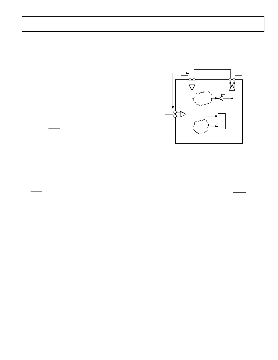
ZERO DELAY OPERATION
Zero delay operation aligns the phase of the output clocks with
the phase of the external PLL reference input. The OUT0 output
is designed to be used as the output for zero delay. There are
two zero delay modes on the AD9524: internal and external (see
Figure 29). Note that the external delay mode provides better
matching than the internal delay mode because the output
drivers are included in the zero delay path. Setting the anitbacklash
pulse width control of PLL1 to maximum gives the best zero
delay matching.
Internal Zero Delay Mode
The internal zero delay function of the AD9524 is achieved
by feeding the output of Channel Divider 0 back to the PLL1
N divider. Bit 5 in Register 0x01B is used to select internal zero
delay mode (see Table 42). In the internal zero delay mode, the
output of Channel Divider 0 is routed back to the PLL1 (N divider)
through a mux. PLL1 synchronizes the phase/edge of the output
of Channel Divider 0 with the phase/edge of the reference input.
Because the channel dividers are synchronized to each other,
the outputs of the channel divider are synchronous with the
reference input.
INTERNAL FB
ZD_IN
REFA
AD9523
FEEDBACK
DELAY
REF
DELAY
ENB
PFD
OUT0
ZD_IN
09081-
027
Figure 29. Zero Delay Function
External Zero Delay Mode
The external zero delay function of the AD9524 is achieved by
feeding OUT0 back to the ZD_IN input and, ultimately, back to
the PLL1 N divider. In Figure 29, the change in signal routing
for external zero delay is external to the AD9524.
Bit 5 in Register 0x01B is used to select the external zero delay
mode. In external zero delay mode, OUT0 must be routed back
to PLL1 (the N divider) through the ZD_IN and ZD_IN pins.
PLL1 synchronizes the phase/edge of the feedback output clock
with the phase/edge of the reference input. Because the channel
dividers are synchronized to each other, the clock outputs are
synchronous with the reference input. Both the reference path
delay and the feedback delay from ZD_IN are designed to have
the same propagation delay from the output drivers and PLL
components to minimize the phase offset between the clock
output and the reference input to achieve zero delay.
LOCK DETECT
PLL1 and PLL2 lock detectors issue an unlock condition when
the frequency error is greater than the threshold of the lock
detector. When the PLL is unlocked, there is a random phase
between the reference clock and feedback clock. Due to the
random phase relationship that exists the unlock condition
could take between 215 × TPFD cycles to 1 × TPFD cycles. For a
lock condition it will always take 216 × TPFD to lock, but it could
potentially take 231 × TPFD cycles depending on how big the
phase jump is and when it occurs in relation to the lock detect
restart.
相关PDF资料 |
PDF描述 |
|---|---|
| AD9540BCPZ-REEL7 | IC CLOCK GEN/SYNTHESIZER 48LFCSP |
| AD9547BCPZ-REEL7 | IC CLOCK GEN/SYNCHRONIZR 64LFCSP |
| AD9548BCPZ-REEL7 | IC CLOCK GEN/SYNCHRONIZR 88LFCSP |
| AD9549ABCPZ-REEL7 | IC CLOCK GEN/SYNCHRONIZR 64LFCSP |
| AD9550BCPZ-REEL7 | IC INTEGER-N TRANSLATOR 32-LFCSP |
相关代理商/技术参数 |
参数描述 |
|---|---|
| AD9524BCPZ-REEL7 | 功能描述:IC INTEGER-N CLCK GEN 48LFCSP RoHS:是 类别:集成电路 (IC) >> 时钟/计时 - 专用 系列:- 标准包装:28 系列:- 类型:时钟/频率发生器 PLL:是 主要目的:Intel CPU 服务器 输入:时钟 输出:LVCMOS 电路数:1 比率 - 输入:输出:3:22 差分 - 输入:输出:无/是 频率 - 最大:400MHz 电源电压:3.135 V ~ 3.465 V 工作温度:0°C ~ 85°C 安装类型:表面贴装 封装/外壳:64-TFSOP (0.240",6.10mm 宽) 供应商设备封装:64-TSSOP 包装:管件 |
| AD9525 | 制造商:AD 制造商全称:Analog Devices 功能描述:Low Jitter Clock Generator with Eight LVPECL Outputs |
| AD9525/PCBZ | 功能描述:时钟和定时器开发工具 Evaluation kit 2950MHz VCO installed RoHS:否 制造商:Texas Instruments 产品:Evaluation Modules 类型:Clock Conditioners 工具用于评估:LMK04100B 频率:122.8 MHz 工作电源电压:3.3 V |
| AD9525/PCBZ-VCO | 功能描述:时钟和定时器开发工具 Evaluation kit CRO29508 VCO installed RoHS:否 制造商:Texas Instruments 产品:Evaluation Modules 类型:Clock Conditioners 工具用于评估:LMK04100B 频率:122.8 MHz 工作电源电压:3.3 V |
| AD9525BCPZ | 功能描述:时钟发生器及支持产品 High performance clock distributor Exter RoHS:否 制造商:Silicon Labs 类型:Clock Generators 最大输入频率:14.318 MHz 最大输出频率:166 MHz 输出端数量:16 占空比 - 最大:55 % 工作电源电压:3.3 V 工作电源电流:1 mA 最大工作温度:+ 85 C 安装风格:SMD/SMT 封装 / 箱体:QFN-56 |
发布紧急采购,3分钟左右您将得到回复。