参数资料
| 型号: | AD9540BCPZ |
| 厂商: | Analog Devices Inc |
| 文件页数: | 2/32页 |
| 文件大小: | 0K |
| 描述: | IC CLOCK GENERATOR PLL 48-LFCSP |
| 标准包装: | 1 |
| 类型: | 时钟发生器 |
| PLL: | 是 |
| 输入: | 时钟 |
| 输出: | CML,PECL |
| 电路数: | 1 |
| 比率 - 输入:输出: | 2:2 |
| 差分 - 输入:输出: | 是/是 |
| 频率 - 最大: | 655MHz |
| 除法器/乘法器: | 是/无 |
| 电源电压: | 1.71 V ~ 1.89 V |
| 工作温度: | -40°C ~ 85°C |
| 安装类型: | 表面贴装 |
| 封装/外壳: | 48-VFQFN 裸露焊盘,CSP |
| 供应商设备封装: | 48-LFCSP-VQ(7x7) |
| 包装: | 托盘 |
| 产品目录页面: | 776 (CN2011-ZH PDF) |
第1页当前第2页第3页第4页第5页第6页第7页第8页第9页第10页第11页第12页第13页第14页第15页第16页第17页第18页第19页第20页第21页第22页第23页第24页第25页第26页第27页第28页第29页第30页第31页第32页
AD9540
Rev. A | Page 10 of 32
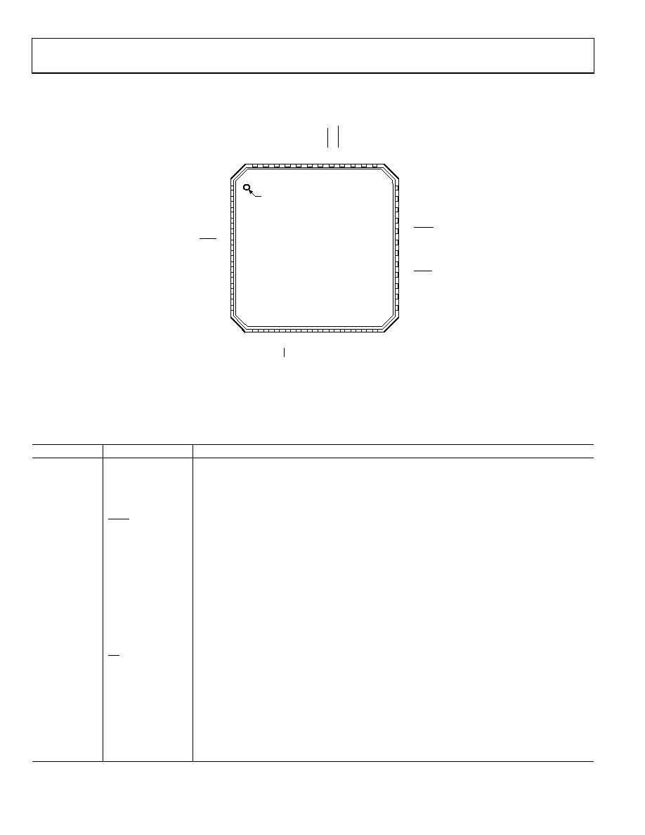
PIN CONFIGURATION AND FUNCTION DESCRIPTIONS
13
14
15
16
17
18
19
20
21
22
23
24
SDO
SDI/O
SCLK
CS
DVDD_
I/O
SYNC_
OUT
SYNC_IN/STATUS
I/O_UPDATE
S0
S1
S2
DGND
48
47
46
45
44
43
42
41
40
39
38
37
AVDD
DAC_
RSE
T
DRV_
R
SET
CP_RSET
AVDD
AGND
CLK2
REFIN
AVDD
AGND
1
2
3
4
5
6
7
8
9
10
11
12
AGND
AVDD
AGND
AVDD
IOUT
AVDD
AGND
I/O_RESET
RESET
DVDD
DGND
CP_VDD
AGND
OUT0
CP_VDD
AGND
CLK1
AVDD
AGND
DVDD
35
CP_OUT
36
34
33
32
31
30
29
28
27
26
25
AD9540
TOP VIEW
(Not to Scale)
PIN 1
INDICATOR
04947-
047
Figure 3. 48-Lead LFCSP Pin Configuration
Table 3. Pin Function Descriptions
Pin No.
Mnemonic
Description
1, 3, 8, 26, 30,
34, 37, 43,
AGND
Analog Ground.
2, 4, 7, 27, 38,
44, 48
AVDD
Analog Core Supply (1.8 V).
5
IOUT
DAC Analog Output.
6
IOUT
DAC Analog Complementary Output.
9
I/O_RESET
Resets the serial port when synchronization is lost in communications but does not reset the
device itself (active high). When not being used, this pin should be forced low, because it floats to
the threshold value.
10
RESET
Master Reset. Clears all accumulators and returns all registers to their default values (active high).
11, 25
DVDD
Digital Core Supply (1.8 V).
12, 24
DGND
Digital Ground.
13
SDO
Serial Data Output. Used only when the device is programmed for 3-wire serial data mode.
14
SDI/O
Serial Data Input/Output. When the part is programmed for 3-wire serial data mode, this is input
only; in 2-wire mode, it serves as both the input and output.
15
SCLK
Serial Data Clock. Provides the clock signal for the serial data port.
16
CS
Active Low Signal That Enables Shared Serial Buses. When brought high, the serial port ignores the
serial data clocks.
17
DVDD_I/O
Digital Interface Supply (3.3 V).
18
SYNC_OUT
Synchronization Clock Output.
19
SYNC_IN/STATUS
Bidirectional Dual Function Pin. Depending on device programming, this pin is either the direct
digital synthesizer’s (DDS) synchronization input (allows alignment of multiple subclocks), or the PLL
lock detect output signal.
20
I/O_UPDATE
This input pin, when set high, transfers the data from the I/O buffers to the internal registers on the
rising edge of the internal SYNC_CLK, which can be observed on SYNC_OUT.
相关PDF资料 |
PDF描述 |
|---|---|
| X9317WM8IZ | IC XDCP SGL 100TAP 10K 8-MSOP |
| X9317UV8IZ | IC XDCP 100TAP 50K 3-WIRE 8TSSOP |
| M83723/76A20257 | CONN PLUG 25POS STRAIGHT W/PINS |
| M83723/76A20256 | CONN PLUG 25POS STRAIGHT W/PINS |
| X9317UM8IZ | IC XDCP 100TAP 10K 3-WIRE 8-MSOP |
相关代理商/技术参数 |
参数描述 |
|---|---|
| AD9540BCPZ-REEL | 制造商:AD 制造商全称:Analog Devices 功能描述:655 MHz Low Jitter Clock Generator |
| AD9540BCPZ-REEL7 | 功能描述:IC CLOCK GEN/SYNTHESIZER 48LFCSP RoHS:是 类别:集成电路 (IC) >> 时钟/计时 - 时钟发生器,PLL,频率合成器 系列:- 标准包装:2,000 系列:- 类型:PLL 时钟发生器 PLL:带旁路 输入:LVCMOS,LVPECL 输出:LVCMOS 电路数:1 比率 - 输入:输出:2:11 差分 - 输入:输出:是/无 频率 - 最大:240MHz 除法器/乘法器:是/无 电源电压:3.135 V ~ 3.465 V 工作温度:0°C ~ 70°C 安装类型:表面贴装 封装/外壳:32-LQFP 供应商设备封装:32-TQFP(7x7) 包装:带卷 (TR) |
| AD9540PCB | 制造商:AD 制造商全称:Analog Devices 功能描述:655 MHz Low Jitter Clock Generator |
| AD9540-VCO/PCB | 制造商:Analog Devices 功能描述:EVAL BD FOR AD9540 ,655 MHZ LOW JITTER CLOCK GEN - Trays |
| AD9540-VCO/PCBZ | 功能描述:BOARD EVAL CLK GEN SYNTH 48LFCSP RoHS:是 类别:编程器,开发系统 >> 评估演示板和套件 系列:- 标准包装:1 系列:- 主要目的:电信,线路接口单元(LIU) 嵌入式:- 已用 IC / 零件:IDT82V2081 主要属性:T1/J1/E1 LIU 次要属性:- 已供物品:板,电源,线缆,CD 其它名称:82EBV2081 |
发布紧急采购,3分钟左右您将得到回复。