- 您现在的位置:买卖IC网 > PDF目录10034 > AD9640ABCPZ-105 (Analog Devices Inc)IC ADC 14BIT 105MSPS 64LFCSP PDF资料下载
参数资料
| 型号: | AD9640ABCPZ-105 |
| 厂商: | Analog Devices Inc |
| 文件页数: | 22/52页 |
| 文件大小: | 0K |
| 描述: | IC ADC 14BIT 105MSPS 64LFCSP |
| 设计资源: | Interfacing ADL5534 to AD9640 High Speed ADC (CN0049) |
| 标准包装: | 1 |
| 位数: | 14 |
| 采样率(每秒): | 105M |
| 数据接口: | 串行,SPI? |
| 转换器数目: | 2 |
| 功率耗散(最大): | 657mW |
| 电压电源: | 模拟和数字 |
| 工作温度: | -40°C ~ 85°C |
| 安装类型: | 表面贴装 |
| 封装/外壳: | 64-VFQFN 裸露焊盘,CSP |
| 供应商设备封装: | 64-LFCSP-VQ(9x9) |
| 包装: | 托盘 |
| 输入数目和类型: | 4 个单端,单极;2 个差分,单极 |
第1页第2页第3页第4页第5页第6页第7页第8页第9页第10页第11页第12页第13页第14页第15页第16页第17页第18页第19页第20页第21页当前第22页第23页第24页第25页第26页第27页第28页第29页第30页第31页第32页第33页第34页第35页第36页第37页第38页第39页第40页第41页第42页第43页第44页第45页第46页第47页第48页第49页第50页第51页第52页
AD9640
Rev. B | Page 29 of 52
CLK+ can be directly driven from a CMOS gate. Although the
CLK+ input circuit supply is AVDD (1.8 V), this input is designed
to withstand input voltages up to 3.6 V, making the selection of
the drive logic voltage very flexible.
OPTIONAL
100
0.1F
39k
50
1
150
RESISTOR IS OPTIONAL
CLK–
CLK+
ADC
AD9640
VCC
1k
1k
CLOCK
INPUT
06547
-038
AD951x
CMOS DRIVER
Figure 60. Single-Ended 1.8 V CMOS Sample Clock (Up to 150 MSPS)
150
RESISTOR IS OPTIONAL
OPTIONAL
100
0.1F
VCC
50
1
CLK–
CLK+
ADC
AD9640
1k
1k
CLOCK
INPUT
06
54
7-
0
39
AD951x
CMOS DRIVER
Figure 61. Single-Ended 3.3 V CMOS Sample Clock (Up to 150 MSPS)
Input Clock Divider
The AD9640 contains an input clock divider with the ability to
divide the input clock by integer values between 1 and 8. If a
divide ratio other than 1 is selected, the duty cycle stabilizer is
automatically enabled.
The AD9640 clock divider can be synchronized using the external
SYNC input. Bit 1 and Bit 2 of Register 0x100 allow the clock
divider to be resynchronized on every SYNC signal or only on
the first SYNC signal after the register is written. A valid SYNC
causes the clock divider to reset to its initial state. This synchro-
nization feature allows multiple parts to have their clock dividers
aligned to guarantee simultaneous input sampling.
Clock Duty Cycle
Typical high speed ADCs use both clock edges to generate
a variety of internal timing signals and, as a result, may be
sensitive to clock duty cycle. Commonly, a ±5% tolerance is
required on the clock duty cycle to maintain dynamic
performance characteristics.
The AD9640 contains a duty cycle stabilizer (DCS) that retimes
the nonsampling (falling) edge, providing an internal clock
signal with a nominal 50% duty cycle. This allows the user to
provide a wide range of clock input duty cycles without affecting
the performance of the AD9640. Noise and distortion performance
are nearly flat for a wide range of duty cycles with the DCS on,
as shown in Figure 43.
Jitter in the rising edge of the input is still of paramount concern
and is not easily reduced by the internal stabilization circuit.
The duty cycle control loop does not function for clock rates
less than 20 MHz nominally. The loop has a time constant
associated with it that needs to be considered where the clock
rate can change dynamically. This requires a wait time of 1.5 μs
to 5 μs after a dynamic clock frequency increase or decrease before
the DCS loop is relocked to the input signal. During the time
period the loop is not locked, the DCS loop is bypassed, and
internal device timing is dependent on the duty cycle of the input
clock signal. In such applications, it may be appropriate to disable
the duty cycle stabilizer. In all other applications, enabling the DCS
circuit is recommended to maximize ac performance.
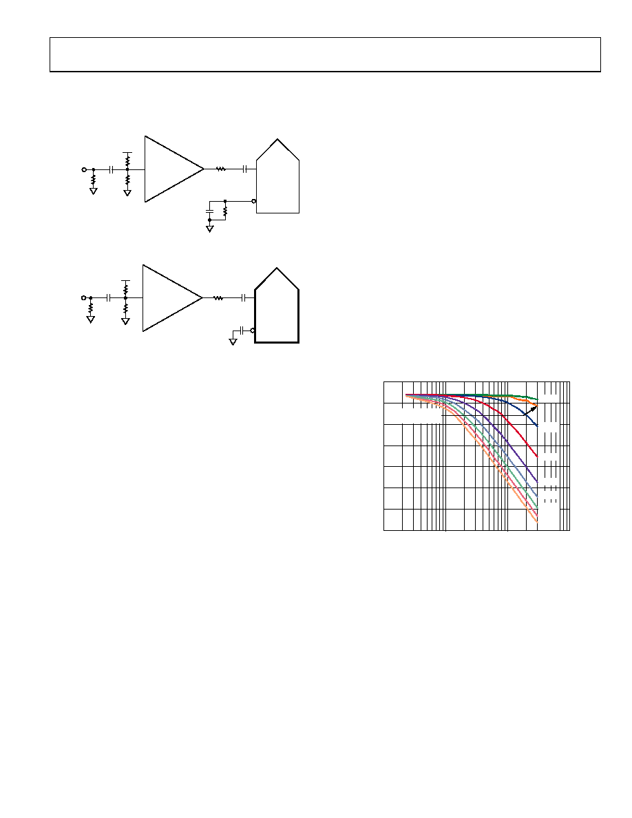
Jitter Considerations
High speed, high resolution ADCs are sensitive to the quality
of the clock input. The degradation in SNR from the low
frequency SNR (SNRLF) at a given input frequency (fINPUT) due
to jitter (tJRMS) can be calculated by
SNRHF = 10 log[(2π × fINPUT × tJRMS)2 + 10
]
)
10
/
(
LF
SNR
In the equation, the rms aperture jitter represents the clock input
jitter specification. IF undersampling applications are particularly
sensitive to jitter, as illustrated in Figure 62.
75
70
65
60
55
50
45
40
1
10
100
1000
S
NR
(
d
Bc)
INPUT FREQUENCY (MHz)
06
54
7-
0
41
3.00ps
0.05ps
MEASURED
PERFORMANCE
0.20ps
0.5ps
1.0ps
1.50ps
2.00ps
2.50ps
Figure 62. SNR vs. Input Frequency and Jitter
The clock input should be treated as an analog signal in cases
where aperture jitter may affect the dynamic range of the AD9640.
Power supplies for clock drivers should be separated from the
ADC output driver supplies to avoid modulating the clock
signal with digital noise. Low jitter, crystal-controlled oscillators
make the best clock sources. If the clock is generated from
another type of source (by gating, dividing, or other methods),
it should be retimed by the original clock at the last step.
See the AN-501 Application Note and AN-756 Application
Note for more information about jitter performance as it
relates to ADCs.
相关PDF资料 |
PDF描述 |
|---|---|
| MS27467E19B11SA | CONN PLUG 11POS STRAIGHT W/SCKT |
| IDT72805LB10PF8 | IC FIFO SYNC DUAL 256X18 128TQFP |
| VI-J4B-MX-S | CONVERTER MOD DC/DC 95V 75W |
| VI-25D-MX-F2 | CONVERTER MOD DC/DC 85V 75W |
| LTC1350IG#TRPBF | IC TXRX 3.3V EIA/TIA-562 28-SSOP |
相关代理商/技术参数 |
参数描述 |
|---|---|
| AD9640ABCPZ-125 | 功能描述:IC ADC 14BIT 125MSPS 64LFCSP RoHS:是 类别:集成电路 (IC) >> 数据采集 - 模数转换器 系列:- 产品培训模块:Lead (SnPb) Finish for COTS Obsolescence Mitigation Program 标准包装:250 系列:- 位数:12 采样率(每秒):1.8M 数据接口:并联 转换器数目:1 功率耗散(最大):1.82W 电压电源:模拟和数字 工作温度:-40°C ~ 85°C 安装类型:表面贴装 封装/外壳:48-LQFP 供应商设备封装:48-LQFP(7x7) 包装:管件 输入数目和类型:2 个单端,单极 |
| AD9640ABCPZ-150 | 功能描述:模数转换器 - ADC 14Bit 150Msps Dual 1.8V PB Free ADC RoHS:否 制造商:Analog Devices 通道数量: 结构: 转换速率: 分辨率: 输入类型: 信噪比: 接口类型: 工作电源电压: 最大工作温度: 安装风格: 封装 / 箱体: |
| AD9640ABCPZ-80 | 功能描述:IC ADC 14BIT 80MSPS 64LFCSP RoHS:是 类别:集成电路 (IC) >> 数据采集 - 模数转换器 系列:- 标准包装:1 系列:- 位数:14 采样率(每秒):83k 数据接口:串行,并联 转换器数目:1 功率耗散(最大):95mW 电压电源:双 ± 工作温度:0°C ~ 70°C 安装类型:通孔 封装/外壳:28-DIP(0.600",15.24mm) 供应商设备封装:28-PDIP 包装:管件 输入数目和类型:1 个单端,双极 |
| AD9640ABCPZRL7-105 | 功能描述:模数转换器 - ADC 14Bit 105Msps Dual 1.8V PB Free ADC RoHS:否 制造商:Analog Devices 通道数量: 结构: 转换速率: 分辨率: 输入类型: 信噪比: 接口类型: 工作电源电压: 最大工作温度: 安装风格: 封装 / 箱体: |
| AD9640ABCPZRL7-125 | 功能描述:14 Bit Analog to Digital Converter 2 Input 2 Pipelined 64-LFCSP-VQ (9x9) 制造商:analog devices inc. 系列:- 包装:带卷(TR) 零件状态:在售 位数:14 采样率(每秒):125M 输入数:2 输入类型:差分,单端 数据接口:并联 配置:S/H-ADC 无线电 - S/H:ADC:1:1 A/D 转换器数:2 架构:管线 参考类型:外部, 内部 电压 - 电源,模拟:1.7 V ~ 1.9 V 电压 - 电源,数字:1.7 V ~ 1.9 V 特性:同步采样 工作温度:-40°C ~ 85°C 封装/外壳:64-VFQFN 裸露焊盘,CSP 供应商器件封装:64-LFCSP-VQ(9x9) 标准包装:750 |
发布紧急采购,3分钟左右您将得到回复。