参数资料
| 型号: | AD9726BSVZ |
| 厂商: | Analog Devices Inc |
| 文件页数: | 10/24页 |
| 文件大小: | 0K |
| 描述: | IC DAC 16IT LVDS 400MSPS 80-TQFP |
| 产品培训模块: | Data Converter Fundamentals DAC Architectures |
| 标准包装: | 1 |
| 系列: | TxDAC+® |
| 位数: | 16 |
| 数据接口: | 并联 |
| 转换器数目: | 1 |
| 电压电源: | 模拟和数字 |
| 功率耗散(最大): | 575mW |
| 工作温度: | -40°C ~ 85°C |
| 安装类型: | 表面贴装 |
| 封装/外壳: | 80-TQFP 裸露焊盘 |
| 供应商设备封装: | 80-TQFP-EP(12x12) |
| 包装: | 托盘 |
| 输出数目和类型: | 2 电流,单极 |
| 采样率(每秒): | 400M |
| 产品目录页面: | 785 (CN2011-ZH PDF) |
| 配用: | AD9726-EBZ-ND - BOARD EVAL FOR AD9726 |
AD9726
Rev. B | Page 18 of 24
The 50 Ω termination resistor should be placed as close as pos-
sible to the input pins, and controlled impedance PCB traces
should be used.
Good ac performance can be expected from either the active or
passive DAC clock drive circuit. However, in a passive circuit,
the output slew rate is dependent on the frequency of the input;
whereas an active circuit provides consistently high output slew
rates over a wide range of input frequencies.
DATA SYNCHRONIZATION CIRCUITRY
The high performance of the AD9726 requires maintaining
synchronization between the incoming bits and the DAC clock
used to sample and convert the data. Despite the inherent dif-
ficulty in specifying the phase relationship of the DAC clock
and the LVDS data clock input and the challenge presented by
the high operating speed of the interface, the AD9726 contains
real-time logic to automatically monitor and align the data bus
with the DAC clock.
Whether in SDR or DDR mode, input data is always provided
at the same rate. Furthermore, the rate of incoming data always
equals the frequency period of the DAC clock. The data rate and
the DAC clock must also be frequency locked. To accomplish this,
the primary purpose of the data clock output is to provide a
time base for data that is derived directly from the DAC clock.
The function of the data clock input is to latch incoming data
into the sync block. From there, it is the function of the
synchronization logic to position the data with respect to the
DAC clock for optimal ac performance.
Individual data bits must maintain close alignment with one
another so that PCB traces have matched delays across the
width of the 16-bit bus. In addition, a fixed setup and hold
timing relationship between the data clock input and the data
bus is required.
However, because of the sync logic, the phase relationship between
the data bus and the DAC clock is internally optimized.
Furthermore, if the phase between the data bus and the DAC
clock drifts over time or temperature, the sync logic automat-
ically updates and adjusts for it. After synchronization is
reached, the phase between the data bus and the DAC clock can
vary by a full cycle without loss or corruption of data.
More detailed explanations of sync operation and optional
programmable modes are presented in the Sync Logic
Operation and Programming section, which also includes an
explanation of how to use the sync logic without the SPI.
Data Synchronization Circuitry Bypass
Due to internal design limitations, the data synchronization
circuitry does not assure a fixed or predictable pipeline delay
between the data input and the analog output after power-up.
For designs where multichip synchronization or fixed pipeline
delay is important, the AD9726 can be configured to bypass the
resynchronization circuitry and assure a fixed pipeline delay of
four DAC clock cycles. In this mode, the data is sampled into
the DAC using the DAC clock (CLK±) and following the timing
The data synchronization circuitry bypass is enabled by writing
0x40 to Address 0x16. The AD9726 should also be configured
in single data rate mode by writing 0x80 to Address 0x02. In this
mode, the sync logic is bypassed, making its configurations and
status reporting irrelevant.
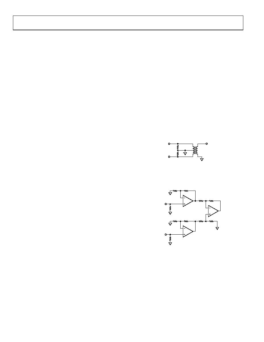
ANALOG OUTPUT
The AD9726 is based around a high dynamic range CMOS
core. The analog output consists of differential current sources,
each capable of up to 20 mA full scale. Discrete output devices
are PMOS and capable of sourcing current into an output
termination within a compliance voltage range of ±1 V.
In a typical application, both outputs drive discrete resistors-to-
analog ground. From there, especially for higher frequency
outputs, they feed the center-tap secondary of a 1:1 RF trans-
former. A differential-to-single-ended conversion is accomplished
that provides added gain and cancellation of even ordered
harmonics.
25
–3dBm
25
IOUTA
IOUTB
04
54
0-
02
1
Figure 21. Transformer Output Circuit
For maximum output power, resistor values can be increased to
50 Ω to provide up to 0 dBm into a 50 Ω load without loss of
performance for most transformers.
04
54
0-
01
1
RGA
50
IOUTA
RFA
RGB
50
IOUTB
RFB
NOTES
1. USE RF AND RG TO SET GAIN
AND LIMIT BANDWIDTH
Figure 22. Op Amp Output Circuit
As an alternative, an active output stage can be used in the
classic instrumentation amplifier configuration. Here, each
DAC output feeds the noninverting input of one of the Analog
Devices, Inc., high speed transimpedance op amps.
相关PDF资料 |
PDF描述 |
|---|---|
| VI-B4Y-MU-F1 | CONVERTER MOD DC/DC 3.3V 132W |
| ICS843004AGI-04LFT | IC SYNTHESIZER LVPECL 24-TSSOP |
| AD569KNZ | IC DAC 16BIT MONOTONIC 28-DIP |
| VI-B4X-MV-F4 | CONVERTER MOD DC/DC 5.2V 150W |
| MS3456L32-17PW | CONN PLUG 4POS STRAIGHT W/PINS |
相关代理商/技术参数 |
参数描述 |
|---|---|
| AD9726BSVZRL | 功能描述:IC DAC 16IT LVDS 400MSPS 80-TQFP RoHS:是 类别:集成电路 (IC) >> 数据采集 - 数模转换器 系列:TxDAC+® 产品培训模块:Lead (SnPb) Finish for COTS Obsolescence Mitigation Program 标准包装:1,000 系列:- 设置时间:1µs 位数:8 数据接口:串行 转换器数目:8 电压电源:双 ± 功率耗散(最大):941mW 工作温度:0°C ~ 70°C 安装类型:表面贴装 封装/外壳:24-SOIC(0.295",7.50mm 宽) 供应商设备封装:24-SOIC W 包装:带卷 (TR) 输出数目和类型:8 电压,单极 采样率(每秒):* |
| AD9726-EB | 制造商:Analog Devices 功能描述:EVAL FOR AD9726 - Bulk |
| AD9726-EBZ | 功能描述:BOARD EVAL FOR AD9726 RoHS:是 类别:编程器,开发系统 >> 评估板 - 数模转换器 (DAC) 系列:TxDAC+® 产品培训模块:Lead (SnPb) Finish for COTS Obsolescence Mitigation Program 标准包装:1 系列:- DAC 的数量:4 位数:12 采样率(每秒):- 数据接口:串行,SPI? 设置时间:3µs DAC 型:电流/电压 工作温度:-40°C ~ 85°C 已供物品:板 已用 IC / 零件:MAX5581 |
| AD972A | 制造商:Analog Devices 功能描述:- Bulk |
| AD9731 | 制造商:AD 制造商全称:Analog Devices 功能描述:10-Bit, 170 MSPS D/A Converter |
发布紧急采购,3分钟左右您将得到回复。