参数资料
| 型号: | AD9726BSVZ |
| 厂商: | Analog Devices Inc |
| 文件页数: | 9/24页 |
| 文件大小: | 0K |
| 描述: | IC DAC 16IT LVDS 400MSPS 80-TQFP |
| 产品培训模块: | Data Converter Fundamentals DAC Architectures |
| 标准包装: | 1 |
| 系列: | TxDAC+® |
| 位数: | 16 |
| 数据接口: | 并联 |
| 转换器数目: | 1 |
| 电压电源: | 模拟和数字 |
| 功率耗散(最大): | 575mW |
| 工作温度: | -40°C ~ 85°C |
| 安装类型: | 表面贴装 |
| 封装/外壳: | 80-TQFP 裸露焊盘 |
| 供应商设备封装: | 80-TQFP-EP(12x12) |
| 包装: | 托盘 |
| 输出数目和类型: | 2 电流,单极 |
| 采样率(每秒): | 400M |
| 产品目录页面: | 785 (CN2011-ZH PDF) |
| 配用: | AD9726-EBZ-ND - BOARD EVAL FOR AD9726 |
AD9726
Rev. B | Page 17 of 24
THEORY OF OPERATION
The AD9726 uses LVDS for input data to enable high sample
rates and high performance. LVDS technology uses differential
signals for noise rejection and small signal amplitude for fast
speed with lower power. Each LVDS input on the AD9726 has
an internal 100 Ω active load for proper termination.
DAC CLOCK AND DATA CLOCK OUTPUT
The AD9726 uses two clock inputs and offers one clock output.
All are differential signals.
The AD9726 is driven by a master input clock that initiates con-
version and controls all on-chip activity. This signal is referred
to as the DAC clock. It is not LVDS, and the CLK+ and CLK–
pins are high impedance inputs.
The DAC clock is then used to generate the data clock output.
The DCLK_OUT+ and DCLK_OUT– pins form an LVDS
signal that can be used to drive an external FPGA or another
data pump. In SDR mode, the data clock output always runs at
the same frequency as the DAC clock. In DDR mode, the data
clock output always runs at the DAC clock frequency.
Use of the data clock output is optional. It is meant to serve as
a convenient means of regulating the incoming data stream.
The driver can be loaded by a 100 Ω differential termination.
An external 1 kΩ resistor from the REXT pin to DBGND is also
required to set the drive strength. If unused, the data clock
output pins can be left unconnected, and the 1 kΩ resistor at
REXT can be omitted.
The data clock output can also be inverted by asserting the
INVDCLKO bit in SPI Register 0x02, or the driver can be
disabled by asserting the DISDCLKO bit in the same register.
DATA CLOCK INPUT
The remaining clock signal associated with the AD9726 is the
data clock input. This LVDS signal is not optional and must
accompany the 16-bit data bus. The data clock input is used to
latch incoming data into the synchronization (sync) logic.
The data clock input always runs at the same frequency as the
data clock output in both SDR and DDR modes. A logical
inversion can be accomplished by asserting the INVDCLKI bit.
Driving the DAC Clock Inputs
The DAC clock must be precise and spectrally pure to ensure
the highest ac performance. A symmetrical 50% duty cycle
should be maintained at all times.
The CLK+ and CLK– input pins should be driven by a signal
with a common-mode voltage near of CLKVDD. From this
point, peak-to-peak signal amplitude should swing over a range
of at least several hundred millivolts.
04540-012
CLK+
VCC – 2V
MC100LVEP16
VCC = CLKVDD = 2.5V
VBB = 1.0V
1:1
50
Ω
50
Ω
CLK–
AD9726
25
Ω
25
Ω
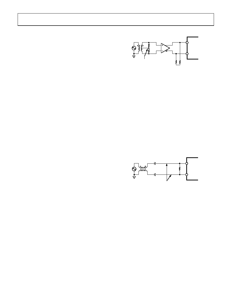
Figure 19. Active DAC Clock Drive Circuit
The circuit option shown in Figure 19 uses a receiver/driver IC
from the 2.5 V LVPECL logic family to provide complementary
outputs that fall within these guidelines. A transformer helps
ensure a 50% duty cycle and provides a single-ended to differ-
ential conversion at the input.
The LVPECL device can be conveniently powered from the
same power supply as CLKVDD. The center tap of the trans-
former secondary must be held at 1 V, the switching threshold
of the receiver/driver inputs (use a resistive divider to generate
this voltage or use the internal VBB source with a buffer
amplifier). Based on a 1:1 impedance ratio, 25 Ω resistors across
the secondary provide a matched load to a 50 Ω source.
The driver outputs are terminated as close as possible to the
AD9726 with 50 Ω to VCC 2 V (or use a Thevenin equivalent
circuit). Controlled impedance PCB traces should be used to
minimize reflections. Signal levels at the CLK+ and CLK– pins
transition between a high near 1500 mV to a low near 750 mV.
0.1
μF
0.1
μF
04540-013
CLK+
VDC BIAS = 1.25V
1:1
50
Ω
CLK–
AD9726
Figure 20. Passive DAC Clock Drive Circuit
An alternative circuit option for driving the DAC clock inputs
employs a transmission line transformer (balun) to accomplish
the single-ended to differential conversion. This all-passive
circuit is considerably simpler and less costly, and it provides
acceptable performance over a limited range of frequencies.
In this implementation, a sine wave (or other single-ended
source) is coupled directly to the differential DAC clock inputs
through a 50 Ω transformer. Capacitors are used for isolation,
and each DAC clock pin must be dc-biased to a level of 1.25 V
(a pair of simple resistive dividers can be used).
相关PDF资料 |
PDF描述 |
|---|---|
| VI-B4Y-MU-F1 | CONVERTER MOD DC/DC 3.3V 132W |
| ICS843004AGI-04LFT | IC SYNTHESIZER LVPECL 24-TSSOP |
| AD569KNZ | IC DAC 16BIT MONOTONIC 28-DIP |
| VI-B4X-MV-F4 | CONVERTER MOD DC/DC 5.2V 150W |
| MS3456L32-17PW | CONN PLUG 4POS STRAIGHT W/PINS |
相关代理商/技术参数 |
参数描述 |
|---|---|
| AD9726BSVZRL | 功能描述:IC DAC 16IT LVDS 400MSPS 80-TQFP RoHS:是 类别:集成电路 (IC) >> 数据采集 - 数模转换器 系列:TxDAC+® 产品培训模块:Lead (SnPb) Finish for COTS Obsolescence Mitigation Program 标准包装:1,000 系列:- 设置时间:1µs 位数:8 数据接口:串行 转换器数目:8 电压电源:双 ± 功率耗散(最大):941mW 工作温度:0°C ~ 70°C 安装类型:表面贴装 封装/外壳:24-SOIC(0.295",7.50mm 宽) 供应商设备封装:24-SOIC W 包装:带卷 (TR) 输出数目和类型:8 电压,单极 采样率(每秒):* |
| AD9726-EB | 制造商:Analog Devices 功能描述:EVAL FOR AD9726 - Bulk |
| AD9726-EBZ | 功能描述:BOARD EVAL FOR AD9726 RoHS:是 类别:编程器,开发系统 >> 评估板 - 数模转换器 (DAC) 系列:TxDAC+® 产品培训模块:Lead (SnPb) Finish for COTS Obsolescence Mitigation Program 标准包装:1 系列:- DAC 的数量:4 位数:12 采样率(每秒):- 数据接口:串行,SPI? 设置时间:3µs DAC 型:电流/电压 工作温度:-40°C ~ 85°C 已供物品:板 已用 IC / 零件:MAX5581 |
| AD972A | 制造商:Analog Devices 功能描述:- Bulk |
| AD9731 | 制造商:AD 制造商全称:Analog Devices 功能描述:10-Bit, 170 MSPS D/A Converter |
发布紧急采购,3分钟左右您将得到回复。