- 您现在的位置:买卖IC网 > PDF目录11768 > AD9883ABSTZ-RL110 (Analog Devices Inc)IC INTERFACE FLAT 110MHZ 80LQFP PDF资料下载
参数资料
| 型号: | AD9883ABSTZ-RL110 |
| 厂商: | Analog Devices Inc |
| 文件页数: | 15/28页 |
| 文件大小: | 0K |
| 描述: | IC INTERFACE FLAT 110MHZ 80LQFP |
| 标准包装: | 1 |
| 应用: | 显示器,监控器,电视 |
| 接口: | 模拟 |
| 电源电压: | 3 V ~ 3.6 V |
| 封装/外壳: | 80-LQFP |
| 供应商设备封装: | 80-LQFP(14x14) |
| 包装: | 标准包装 |
| 安装类型: | 表面贴装 |
| 其它名称: | AD9883ABSTZ-RL110DKR |
第1页第2页第3页第4页第5页第6页第7页第8页第9页第10页第11页第12页第13页第14页当前第15页第16页第17页第18页第19页第20页第21页第22页第23页第24页第25页第26页第27页第28页
REV. B
AD9883A
–22–
Table XXXIV. Detected Coast Input Polarity Status
Polarity Status
Result
0Coast Polarity Negative
1Coast Polarity Positive
This indicates that Bit 1 of Register 5 is the 4:2:2 Output
mode select bit.
15
1
4:2:2 Output Mode Select
A bit that configures the output data in 4:2:2 mode.
This mode can be used to reduce the number of data
lines used from 24 down to 16 for applications using
YUV, YCbCr, or YPbPr graphics signals. A timing
diagram for this mode is shown in Figure 9.
Recommended input and output configurations are
shown in Table XXXV.
Table XXXV. 4:2:2 Output Mode Select
Select
Output Mode
0
4:2:2
1
4:4:4
Table XXXVI. 4:2:2 Input/Output Configuration
Input
Channel
Connection
Output Format
Red
V
U/V
Green
Y
Blue
U
High Impedance
2-WIRE SERIAL CONTROL PORT
A 2-wire serial interface control interface is provided. Up to two
AD9883A devices may be connected to the 2-wire serial interface,
with each device having a unique address.
The 2-wire serial interface comprises a clock (SCL) and a bidi-
rectional data (SDA) pin. The analog flat panel interface acts as
a slave for receiving and transmitting data over the serial interface.
When the serial interface is not active, the logic levels on SCL
and SDA are pulled high by external pull-up resistors.
Data received or transmitted on the SDA line must be stable for
the duration of the positive-going SCL pulse. Data on SDA must
change only when SCL is low. If SDA changes state while SCL
is high, the serial interface interprets that action as a start or
stop sequence.
There are five components to serial bus operation:
Start Signal
Slave Address Byte
Base Register Address Byte
Data Byte to Read or Write
Stop Signal
When the serial interface is inactive (SCL and SDA are high)
communications are initiated by sending a start signal. The start
signal is a high-to-low transition on SDA while SCL is high.
This signal alerts all slaved devices that a data transfer sequence
is coming.
The first eight bits of data transferred after a start signal com-
prise a 7-bit slave address (the first seven bits) and a single R/
W
Bit (the eighth bit). The R/
W Bit indicates the direction of data
transfer, read from (1) or write to (0) the slave device. If the
transmitted slave address matches the address of the device (set by
the state of the SA1-0 input pins in Table XXXIV, the AD9883A
acknowledges by bringing SDA low on the ninth SCL pulse. If the
addresses do not match, the AD9883A does not acknowledge.
Table XXXVII. Serial Port Addresses
Bit 7
Bit 6
Bit 5
Bit 4
Bit 3
Bit 2
Bit 1
A6
A5
A4
A3
A2
A1
A0
(MSB)
10
01100
10
01101
Data Transfer via Serial Interface
For each byte of data read or written, the MSB is the first bit of
the sequence.
If the AD9883A does not acknowledge the master device during
a write sequence, the SDA remains high so the master can gen-
erate a stop signal. If the master device does not acknowledge the
AD9883A during a read sequence, the AD9883A interprets this
as “end of data.” The SDA remains high so the master can
generate a stop signal.
Writing data to specific control registers of the AD9883A requires
that the 8-bit address of the control register of interest be written
after the slave address has been established. This control register
address is the base address for subsequent write operations. The
base address autoincrements by one for each byte of data written
after the data byte intended for the base address. If more bytes
are transferred than there are available addresses, the address will
not increment and remains at its maximum value of 14H. Any base
address higher than 14H will not produce an acknowledge signal.
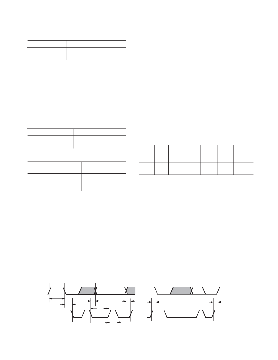
SDA
SCL
tBUFF
tSTAH
tDHO
tDSU
tDAL
tDAH
tSTASU
tSTOSU
Figure 10. Serial Port Read/Write Timing
相关PDF资料 |
PDF描述 |
|---|---|
| VI-B42-IW-F1 | CONVERTER MOD DC/DC 15V 100W |
| PIC12C509-04I/P | IC MCU OTP 1KX12 8DIP |
| D38999/24WC4PA | CONN RCPT 4POS JAM NUT W/PINS |
| PIC16LF1507-E/P | IC MCU 8BIT 3.5KB FLASH 20PDIP |
| VI-B41-IX-F4 | CONVERTER MOD DC/DC 12V 75W |
相关代理商/技术参数 |
参数描述 |
|---|---|
| AD9883ABSTZ-RL140 | 功能描述:IC INTERFACE FLAT 140MHZ 80LQFP RoHS:是 类别:集成电路 (IC) >> 接口 - 专用 系列:- 标准包装:3,000 系列:- 应用:PDA,便携式音频/视频,智能电话 接口:I²C,2 线串口 电源电压:1.65 V ~ 3.6 V 封装/外壳:24-WQFN 裸露焊盘 供应商设备封装:24-QFN 裸露焊盘(4x4) 包装:带卷 (TR) 安装类型:表面贴装 产品目录页面:1015 (CN2011-ZH PDF) 其它名称:296-25223-2 |
| AD9883AKST-1 | 制造商:Analog Devices 功能描述: |
| AD9883AKST-110 | 制造商:Analog Devices 功能描述:ADC Triple 110Msps 8-bit Parallel 80-Pin LQFP 制造商:Rochester Electronics LLC 功能描述:110MHZ ANALOG INTERFACE FOR SGA FPD - Bulk 制造商:Analog Devices 功能描述:IC INTERFACE GRAPHIC |
| AD9883AKST-140 | 制造商:Analog Devices 功能描述:ADC Triple 140Msps 8-bit Parallel 80-Pin LQFP 制造商:Analog Devices 功能描述:IC INTERFACE ANALOG |
| AD9883AKSTZ-110 | 功能描述:IC FLAT PANEL INTERFACE 80-LQFP RoHS:是 类别:集成电路 (IC) >> 接口 - 专用 系列:- 特色产品:NXP - I2C Interface 标准包装:1 系列:- 应用:2 通道 I²C 多路复用器 接口:I²C,SM 总线 电源电压:2.3 V ~ 5.5 V 封装/外壳:16-TSSOP(0.173",4.40mm 宽) 供应商设备封装:16-TSSOP 包装:剪切带 (CT) 安装类型:表面贴装 产品目录页面:825 (CN2011-ZH PDF) 其它名称:568-1854-1 |
发布紧急采购,3分钟左右您将得到回复。