参数资料
| 型号: | AD9949KCPZ |
| 厂商: | Analog Devices Inc |
| 文件页数: | 10/36页 |
| 文件大小: | 0K |
| 描述: | IC CCD SIGNAL PROCESSOR 40-LFCSP |
| 标准包装: | 1 |
| 类型: | CCD 信号处理器,12 位 |
| 输入类型: | 逻辑 |
| 输出类型: | 逻辑 |
| 接口: | 3 线串口 |
| 安装类型: | 表面贴装 |
| 封装/外壳: | 40-VFQFN 裸露焊盘,CSP |
| 供应商设备封装: | 40-LFCSP |
| 包装: | 托盘 |
第1页第2页第3页第4页第5页第6页第7页第8页第9页当前第10页第11页第12页第13页第14页第15页第16页第17页第18页第19页第20页第21页第22页第23页第24页第25页第26页第27页第28页第29页第30页第31页第32页第33页第34页第35页第36页
AD9949
Rev. B | Page 18 of 36
PRECISION TIMING HIGH SPEED TIMING GENERATION
The AD9949 generates flexible high speed timing signals using
the Precision Timing core. This core is the foundation for gener-
ating the timing used for both the CCD and the AFE: the reset
gate (RG), horizontal drivers (H1 to H4), and the SHP/SHD
sample clocks. A unique architecture makes it routine for the
system designer to optimize image quality by providing precise
control over the horizontal CCD readout and the AFE corre-
lated double sampling.
TIMING RESOLUTION
The Precision Timing core uses a 1× master clock input (CLI) as
a reference. This clock should be the same as the CCD pixel
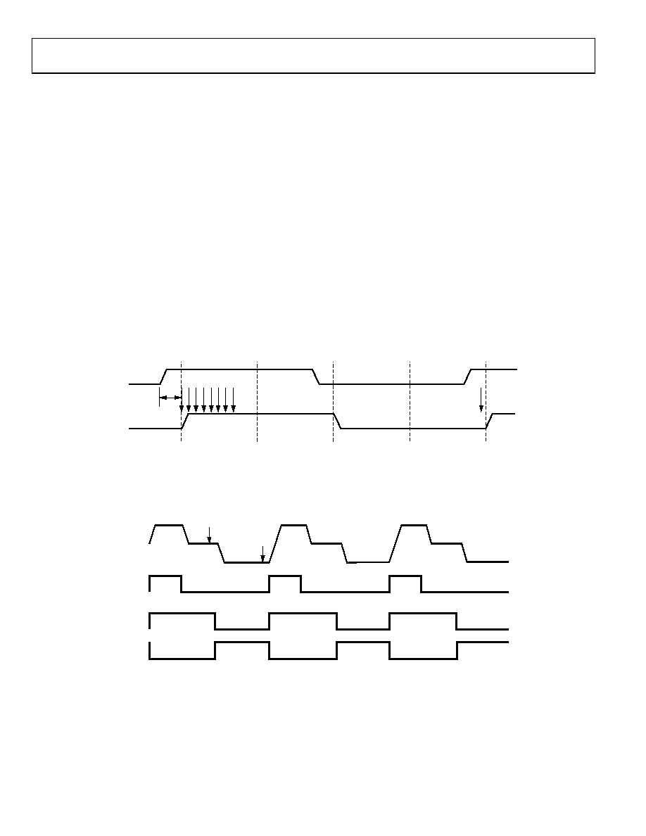
clock frequency. Figure 16 illustrates how the internal timing
core divides the master clock period into 48 steps or edge
positions. Therefore, the edge resolution of the Precision Timing
core is (tCLI/48). For more information on using the CLI input,
refer to the Applications Information section.
HIGH SPEED CLOCK PROGRAMMABILITY
Figure 17 shows how the high speed clocks, RG, H1 to H4,
SHP, and SHD, are generated. The RG pulse has programma-
ble rising and falling edges and may be inverted using the
polarity control. The horizontal clocks H1 and H3 have
programmable rising and falling edges and polarity control.
The H2 and H4 clocks are always inverses of H1 and H3, re-
spectively. Table 16 summarizes the high speed timing registers
and their parameters.
Each edge location setting is 6 bits wide, but only 48 valid edge
locations are available. Therefore, the register values are
mapped into four quadrants, with each quadrant containing
12 edge locations. Table 17 shows the correct register values for
the corresponding edge locations.
NOTES
1. PIXEL CLOCK PERIOD IS DIVIDED INTO 48 POSITIONS, PROVIDING FINE EDGE RESOLUTION FOR HIGH SPEED CLOCKS.
2. THERE IS A FIXED DELAY FROM THE CLI INPUT TO THE INTERNAL PIXEL PERIOD POSITIONS (
tCLIDLY = 6 ns TYP).
P[0]
P[48] = P[0]
P[12]
P[24]
P[36]
1 PIXEL
PERIOD
...
CLI
tCLIDLY
POSITION
03751-017
Figure 16. High Speed Clock Resolution from CLI Master Clock Input
H1/H3
H2/H4
CCD SIGNAL
RG
12
3
4
56
PROGRAMMABLE CLOCK POSITIONS:
1. RG RISING EDGE.
2. RG FALLING EDGE.
3. SHP SAMPLE LOCATION.
4. SHD SAMPLE LOCATION.
5. H1/H3 RISING EDGE POSITION6. H1/H3 FALLING EDGE POSITION (H2/H4 ARE INVERSE OF H1/H3).
03751-018
Figure 17. High Speed Clock Programmable Locations
相关PDF资料 |
PDF描述 |
|---|---|
| AD9951YSVZ | IC DDS DAC 14BIT 1.8V 48-TQFP |
| AD9952YSVZ-REEL7 | IC DDS DAC 14BIT 1.8V 48TQFP |
| AD9953YSVZ-REEL7 | IC DDS DAC 14BIT 1.8V 48TQFP |
| AD9954YSVZ-REEL7 | IC DDS DAC 14BIT 1.8V 48TQFP |
| AD9956YCPZ-REEL7 | IC SYNTHESIZER 1.8V 48LFCSP |
相关代理商/技术参数 |
参数描述 |
|---|---|
| AD9949KCPZRL | 功能描述:IC CCD SIGNAL PROCESSOR 40-LFCSP RoHS:是 类别:集成电路 (IC) >> 接口 - 传感器和探测器接口 系列:- 其它有关文件:Automotive Product Guide 产品培训模块:Lead (SnPb) Finish for COTS Obsolescence Mitigation Program 标准包装:74 系列:- 类型:触控式传感器 输入类型:数字 输出类型:数字 接口:JTAG,串行 电流 - 电源:100µA 安装类型:表面贴装 封装/外壳:20-TSSOP(0.173",4.40mm 宽) 供应商设备封装:20-TSSOP 包装:管件 |
| AD9950KJ | 制造商:未知厂家 制造商全称:未知厂家 功能描述:Parallel-Input Frequency Synthesizer |
| AD9950TJ | 制造商:未知厂家 制造商全称:未知厂家 功能描述:Parallel-Input Frequency Synthesizer |
| AD9951 | 制造商:AD 制造商全称:Analog Devices 功能描述:400 MSPS 14-Bit, 1.8 V CMOS Direct Digital Synthesizer |
| AD9951/PCBZ | 制造商:Analog Devices 功能描述:AD9951 400 MSPS DDS W/ 14 BIT DAC EVALBD - Boxed Product (Development Kits) |
发布紧急采购,3分钟左右您将得到回复。