参数资料
| 型号: | AD9949KCPZ |
| 厂商: | Analog Devices Inc |
| 文件页数: | 4/36页 |
| 文件大小: | 0K |
| 描述: | IC CCD SIGNAL PROCESSOR 40-LFCSP |
| 标准包装: | 1 |
| 类型: | CCD 信号处理器,12 位 |
| 输入类型: | 逻辑 |
| 输出类型: | 逻辑 |
| 接口: | 3 线串口 |
| 安装类型: | 表面贴装 |
| 封装/外壳: | 40-VFQFN 裸露焊盘,CSP |
| 供应商设备封装: | 40-LFCSP |
| 包装: | 托盘 |
第1页第2页第3页当前第4页第5页第6页第7页第8页第9页第10页第11页第12页第13页第14页第15页第16页第17页第18页第19页第20页第21页第22页第23页第24页第25页第26页第27页第28页第29页第30页第31页第32页第33页第34页第35页第36页
AD9949
Rev. B | Page 12 of 36
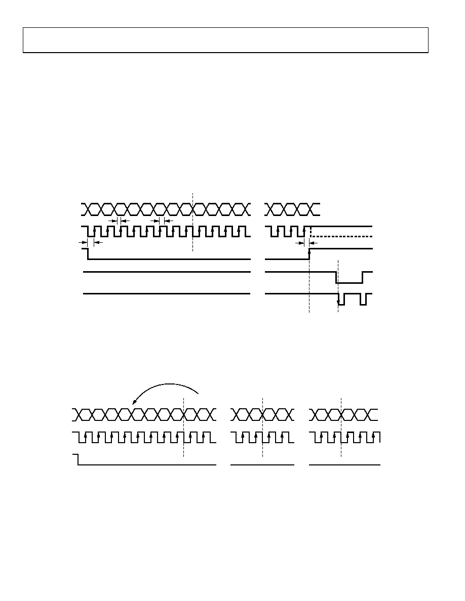
SERIAL INTERFACE TIMING
The AD9949’s internal registers are accessed through a 3-wire
serial interface. Each register consists of an 8-bit address and a
24-bit data-word. Both the 8-bit address and 24-bit data-word
are written starting with the LSB. To write to each register, a
32-bit operation is required, as shown in Figure 14. Although
many registers are less than 24 bits wide, all 24 bits must be
written for each register. If the register is only 16 bits wide, then
the upper eight bits may be filled with zeros during the serial
write operation. If fewer than 24 bits are written, the register
will not be updated with new data.
Figure 15 shows a more efficient way to write to the registers by
using the AD9949’s address auto-increment capability. Using
this method, the lowest desired address is written first, followed
by multiple 24-bit data-words. Each new 24-bit data-word is
written automatically to the next highest register address. By
eliminating the need to write each 8-bit address, faster register
loading is achieved. Address auto-increment may be used start-
ing with any register location and may be used to write to as few
as two registers or as many as the entire register space.
SDATA
A0
A1
A2
A4
A5
A6
A7
D0
D1
D2
D3
D21
D22
D23
SCK
SL
A3
NOTES
1. INDIVIDUAL SDATA BITS ARE LATCHED ON SCK RISING EDGES.
2. ALL 32 BITS MUST BE WRITTEN: 8 BITS FOR ADDRESS AND 24 BITS FOR DATA.
3. IF THE REGISTER LENGTH IS <24 BITS, THEN DON’T CARE BITS MUST BE USED TO COMPLETE THE 24-BIT DATA LENGTH.
4. NEW DATA IS UPDATED AT EITHER THE SL RISING EDGE OR AT THE HD FALLING EDGE AFTER THE NEXT VD FALLING EDGE.
5. VD/HD UPDATE POSITION MAY BE DELAYED TO ANY HD FALLING EDGE IN THE FIELD USING THE UPDATE REGISTER.
VD
SL UPDATED
VD/HD UPDATED
HD
...
8-BIT ADDRESS
24-BIT DATA
1
32
2
3
4
5
6
7
8
9
10
11
12
30
31
03751-015
tLS
tDS
tDH
tLH
Figure 14. Serial Write Operation
SDATA
A0
A1
A2
A4
A5
A6
A7
D0
D1
D22
D23
SCK
SL
A3
NOTES
1. MULTIPLE SEQUENTIAL REGISTERS MAY BE LOADED CONTINUOUSLY.
2. THE FIRST (LOWEST ADDRESS) REGISTER ADDRESS IS WRITTEN, FOLLOWED BY MULTIPLE 24-BIT DATA-WORDS.
3. THE ADDRESS WILL AUTOMATICALLY INCREMENT WITH EACH 24-BIT DATA-WORD (ALL 24 BITS MUST BE WRITTEN).
4. SL IS HELD LOW UNTIL THE LAST DESIRED REGISTER HAS BEEN LOADED.
5. NEW DATA IS UPDATED AT EITHER THE SL RISING EDGE OR AT THE HD FALLING EDGE AFTER THE NEXT VD FALLING EDGE.
D0
D1
D22
D23
D0
...
DATA FOR STARTING
REGISTER ADDRESS
DATA FOR NEXT
REGISTER ADDRESS
D2
D1
...
1
32
23
45
6
7
89
10
31
34
33
56
55
58
57
59
03751-016
Figure 15. Continuous Serial Write Operation
相关PDF资料 |
PDF描述 |
|---|---|
| AD9951YSVZ | IC DDS DAC 14BIT 1.8V 48-TQFP |
| AD9952YSVZ-REEL7 | IC DDS DAC 14BIT 1.8V 48TQFP |
| AD9953YSVZ-REEL7 | IC DDS DAC 14BIT 1.8V 48TQFP |
| AD9954YSVZ-REEL7 | IC DDS DAC 14BIT 1.8V 48TQFP |
| AD9956YCPZ-REEL7 | IC SYNTHESIZER 1.8V 48LFCSP |
相关代理商/技术参数 |
参数描述 |
|---|---|
| AD9949KCPZRL | 功能描述:IC CCD SIGNAL PROCESSOR 40-LFCSP RoHS:是 类别:集成电路 (IC) >> 接口 - 传感器和探测器接口 系列:- 其它有关文件:Automotive Product Guide 产品培训模块:Lead (SnPb) Finish for COTS Obsolescence Mitigation Program 标准包装:74 系列:- 类型:触控式传感器 输入类型:数字 输出类型:数字 接口:JTAG,串行 电流 - 电源:100µA 安装类型:表面贴装 封装/外壳:20-TSSOP(0.173",4.40mm 宽) 供应商设备封装:20-TSSOP 包装:管件 |
| AD9950KJ | 制造商:未知厂家 制造商全称:未知厂家 功能描述:Parallel-Input Frequency Synthesizer |
| AD9950TJ | 制造商:未知厂家 制造商全称:未知厂家 功能描述:Parallel-Input Frequency Synthesizer |
| AD9951 | 制造商:AD 制造商全称:Analog Devices 功能描述:400 MSPS 14-Bit, 1.8 V CMOS Direct Digital Synthesizer |
| AD9951/PCBZ | 制造商:Analog Devices 功能描述:AD9951 400 MSPS DDS W/ 14 BIT DAC EVALBD - Boxed Product (Development Kits) |
发布紧急采购,3分钟左右您将得到回复。