参数资料
| 型号: | AD9949KCPZ |
| 厂商: | Analog Devices Inc |
| 文件页数: | 22/36页 |
| 文件大小: | 0K |
| 描述: | IC CCD SIGNAL PROCESSOR 40-LFCSP |
| 标准包装: | 1 |
| 类型: | CCD 信号处理器,12 位 |
| 输入类型: | 逻辑 |
| 输出类型: | 逻辑 |
| 接口: | 3 线串口 |
| 安装类型: | 表面贴装 |
| 封装/外壳: | 40-VFQFN 裸露焊盘,CSP |
| 供应商设备封装: | 40-LFCSP |
| 包装: | 托盘 |
第1页第2页第3页第4页第5页第6页第7页第8页第9页第10页第11页第12页第13页第14页第15页第16页第17页第18页第19页第20页第21页当前第22页第23页第24页第25页第26页第27页第28页第29页第30页第31页第32页第33页第34页第35页第36页
AD9949
Rev. B | Page 29 of 36
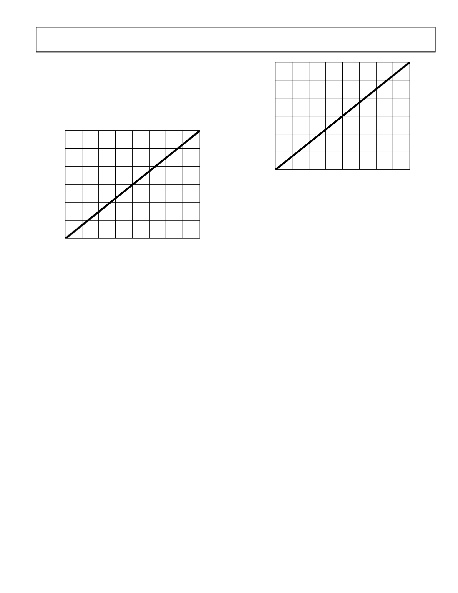
The PxGA gain for each of the four channels is variable from
0 dB to 18 dB in 512 steps, specified using the PxGA GAIN01
and PxGA GAIN23 registers. The PxGA gain curve is shown in
Figure 36. The PxGA GAIN01 register contains nine bits each
for PxGA Gain0 and Gain1, and the PxGA GAIN23 register
contains nine bits each for PxGA Gain2 and Gain3.
PxGA GAIN REGISTER CODE
18
0
PxGA
GAIN
(
d
B)
64
128
192
256
320
384
448
511
15
12
9
6
3
0
03751-037
Figure 36. PxGA Gain Curve
VARIABLE GAIN AMPLIFIER
The VGA stage provides a gain range of 6 dB to 42 dB, pro-
grammable with 10-bit resolution through the serial digital
interface. The minimum gain of 6 dB is needed to match a 1 V
input signal with the ADC full-scale range of 2 V. When com-
pared to 1 V full-scale systems, the equivalent gain range is 0
dB to 36 dB.
The VGA gain curve follows a linear-in-dB characteristic. The
exact VGA gain can be calculated for any gain register value by
using the equation
Gain (db) = (0.0351 × Code) + 6 dB
where the code range is 0 to 1023.
There is a restriction on the maximum amount of gain that can
be applied to the signal. The PxGA can add as much as 18 dB,
and the VGA is capable of providing up to 42 dB. However, the
maximum total gain from the PxGA and VGA is restricted to
42 dB. If the registers are programmed to specify a total gain
higher than 42 dB, the total gain is clipped at 42 dB.
ADC
The AD9949 uses a high performance ADC architecture,
optimized for high speed and low power. DNL performance is
typically better than 0.5 LSB. The ADC uses a 2 V input range.
See Figure 9 and Figure 10 for typical linearity and noise
performance plots for the AD9949.
03751-038
VGA GAIN REGISTER CODE
1023
0
127
255
383
511
639
767
895
V
G
A
GAIN
(dB)
42
36
30
24
18
12
0
Figure 37. VGA Gain Curve (PxGA Not Included)
OPTICAL BLACK CLAMP
The optical black clamp loop is used to remove residual offsets
in the signal chain and to track low frequency variations in the
CCD’s black level. During the optical black (shielded) pixel in-
terval on each line, the ADC output is compared with a fixed
black level reference, selected by the user in the clamp level regis-
ter. The value can be programmed between 0 LSB and 255 LSB
in 256 steps. The resulting error signal is filtered to reduce noise,
and the correction value is applied to the ADC input through a
DAC. Normally, the optical black clamp loop is turned on once
per horizontal line, but this loop can be updated more slowly to
suit a particular application. If external digital clamping is used
during the postprocessing, the AD9949 optical black clamping
may be disabled using Bit D2 in the OPRMODE register. When
the loop is disabled, the clamp level register may still be used to
provide programmable offset adjustment.
The CLPOB pulse should be placed during the CCD’s optical
black pixels. It is recommended that the CLPOB pulse duration
be at least 20 pixels wide to minimize clamp noise. Shorter pulse
widths may be used, but clamp noise may increase and the
ability to track low frequency variations in the black level will
be reduced. See the Horizontal Clamping and Blanking and
Applications Information sections for timing examples.
DIGITAL DATA OUTPUTS
The AD9949 digital output data is latched using the DOUT
phase register value, as shown in Figure 28. Output data timing
is shown in Figure 19 and Figure 20. It is also possible to leave
the output latches transparent, so that the data outputs are valid
immediately from the ADC. Programming the AFE control
register Bit D4 to a 1 sets the output latches transparent. The
data outputs can also be disabled (three-stated) by setting the
AFE control register Bit D3 to a 1.
The data output coding is normally straight binary, but the
coding may be changed to gray coding by setting the AFE
control register Bit D5 to a 1.
相关PDF资料 |
PDF描述 |
|---|---|
| AD9951YSVZ | IC DDS DAC 14BIT 1.8V 48-TQFP |
| AD9952YSVZ-REEL7 | IC DDS DAC 14BIT 1.8V 48TQFP |
| AD9953YSVZ-REEL7 | IC DDS DAC 14BIT 1.8V 48TQFP |
| AD9954YSVZ-REEL7 | IC DDS DAC 14BIT 1.8V 48TQFP |
| AD9956YCPZ-REEL7 | IC SYNTHESIZER 1.8V 48LFCSP |
相关代理商/技术参数 |
参数描述 |
|---|---|
| AD9949KCPZRL | 功能描述:IC CCD SIGNAL PROCESSOR 40-LFCSP RoHS:是 类别:集成电路 (IC) >> 接口 - 传感器和探测器接口 系列:- 其它有关文件:Automotive Product Guide 产品培训模块:Lead (SnPb) Finish for COTS Obsolescence Mitigation Program 标准包装:74 系列:- 类型:触控式传感器 输入类型:数字 输出类型:数字 接口:JTAG,串行 电流 - 电源:100µA 安装类型:表面贴装 封装/外壳:20-TSSOP(0.173",4.40mm 宽) 供应商设备封装:20-TSSOP 包装:管件 |
| AD9950KJ | 制造商:未知厂家 制造商全称:未知厂家 功能描述:Parallel-Input Frequency Synthesizer |
| AD9950TJ | 制造商:未知厂家 制造商全称:未知厂家 功能描述:Parallel-Input Frequency Synthesizer |
| AD9951 | 制造商:AD 制造商全称:Analog Devices 功能描述:400 MSPS 14-Bit, 1.8 V CMOS Direct Digital Synthesizer |
| AD9951/PCBZ | 制造商:Analog Devices 功能描述:AD9951 400 MSPS DDS W/ 14 BIT DAC EVALBD - Boxed Product (Development Kits) |
发布紧急采购,3分钟左右您将得到回复。