参数资料
| 型号: | AD9949KCPZ |
| 厂商: | Analog Devices Inc |
| 文件页数: | 24/36页 |
| 文件大小: | 0K |
| 描述: | IC CCD SIGNAL PROCESSOR 40-LFCSP |
| 标准包装: | 1 |
| 类型: | CCD 信号处理器,12 位 |
| 输入类型: | 逻辑 |
| 输出类型: | 逻辑 |
| 接口: | 3 线串口 |
| 安装类型: | 表面贴装 |
| 封装/外壳: | 40-VFQFN 裸露焊盘,CSP |
| 供应商设备封装: | 40-LFCSP |
| 包装: | 托盘 |
第1页第2页第3页第4页第5页第6页第7页第8页第9页第10页第11页第12页第13页第14页第15页第16页第17页第18页第19页第20页第21页第22页第23页当前第24页第25页第26页第27页第28页第29页第30页第31页第32页第33页第34页第35页第36页
AD9949
Rev. B | Page 30 of 36
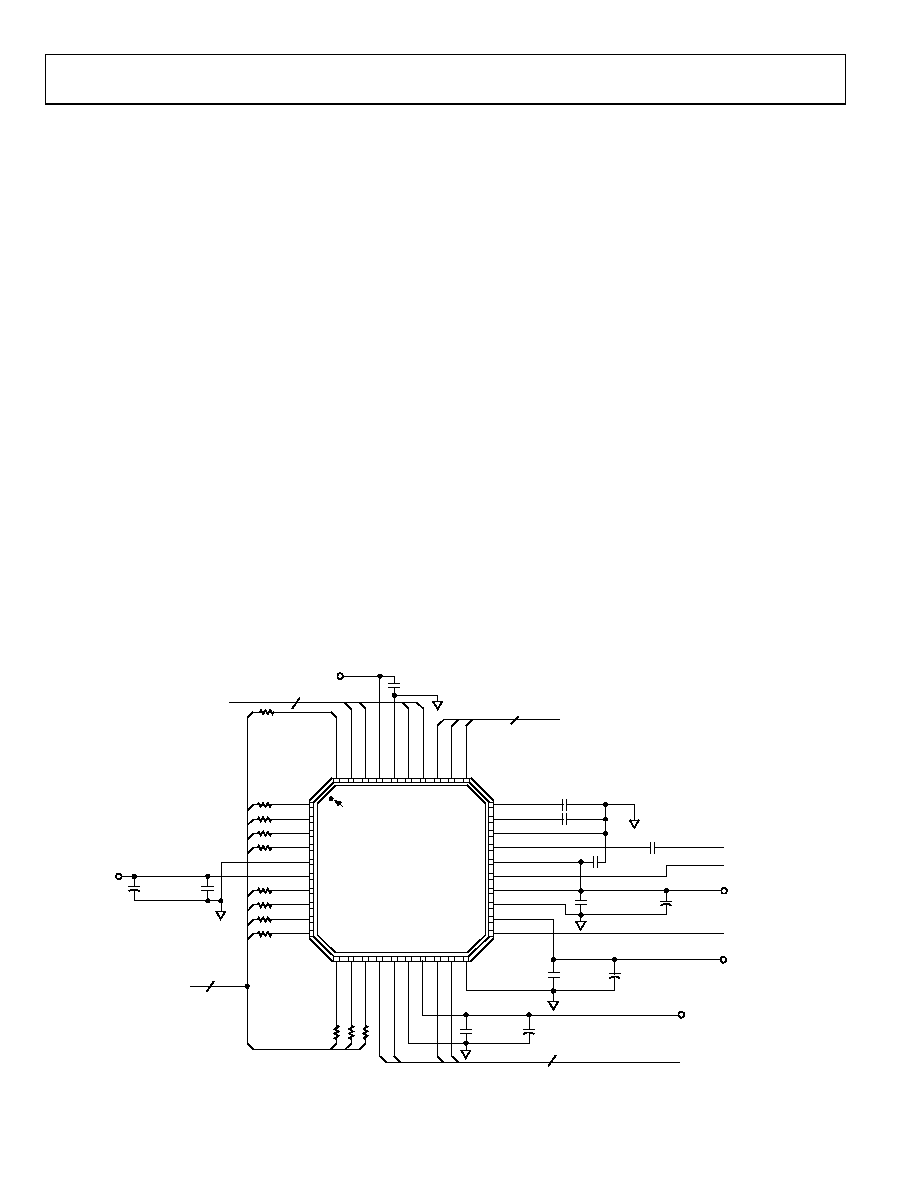
APPLICATIONS INFORMATION
CIRCUIT CONFIGURATION
The AD9949 recommended circuit configuration is shown in
Figure 38. Achieving good image quality from the AD9949
requires careful attention to PCB layout. All signals should be
routed to maintain low noise performance. The CCD output
signal should be directly routed to Pin 27 through a 0.1 F
capacitor. The master clock CLI should be carefully routed to
Pin 25 to minimize interference with the CCDIN, REFT, and
REFB signals.
The digital outputs and clock inputs are located on Pins 1 to 13
and Pins 31 to 40 and should be connected to the digital ASIC
away from the analog and CCD clock signals. Placing series
resistors close to the digital output pins may help to reduce
digital code transition noise. If the digital outputs must drive a
load larger than 20 pF, buffering is recommended to minimize
additional noise. If the digital ASIC can accept gray code, the
AD9949’s outputs can be selected to output data in gray code
format using the control register Bit D5. Gray coding helps reduce
potential digital transition noise compared with binary coding.
The H1–H4 and RG traces should have low inductance to avoid
excessive distortion of the signals. Heavier traces are recom-
mended because of the large transient current demand on
H1–H4 from the capacitive load of the CCD. If possible,
physically locating the AD9949 closer to the CCD will reduce
the inductance on these lines. As always, the routing path
should be as direct as possible from the AD9949 to the CCD.
GROUNDING AND DECOUPLING
RECOMMENDATIONS
As shown in Figure 38, a single ground plane is recommended
for the AD9949. This ground plane should be as continuous as
possible, particularly around Pins 23 to 30. This ensures that all
analog decoupling capacitors provide the lowest possible
impedance path between the power and bypass pins and their
respective ground pins. All high frequency decoupling
capacitors should be located as close as possible to the package
pins. It is recommended that the exposed paddle on the bottom
of the package be soldered to a large pad, with multiple vias
connecting the pad to the ground plane.
All the supply pins must be decoupled to ground with good
quality, high frequency chip capacitors. There should also be a
4.7 F or larger bypass capacitor for each main supply—AVDD,
RGVDD, HVDD, and DRVDD—although this is not necessary
for each individual pin. In most applications, it is easier to share
the supply for RGVDD and HVDD, which may be done as long
as the individual supply pins are separately bypassed. A separate
3 V supply may be used for DRVDD, but this supply pin should
still be decoupled to the same ground plane as the rest of the
chip. A separate ground for DRVSS is not recommended.
The reference bypass pins (REFT, REFB) should be decoupled
to ground as close as possible to their respective pins. The
analog input (CCDIN) capacitor should also be located close to
the pin.
3V ANALOG SUPPLY
SERIAL
INTERFACE
3
CCD SIGNAL
VD/HD/HBLK INPUTS
CLP/BLK OUTPUT
4
3V
DRIVER
SUPPLY
RG DRIVER
SUPPLY
H DRIVER
SUPPLY
MASTER
CLOCK INPUT
3V ANALOG
SUPPLY
DATA
OUTPUTS
12
H1 TO H4
4
TOP VIEW
AD9949
PIN 1
IDENTIFIER
30
REFB
29
REFT
28
AVSS
27
CCDIN
26
AVDD
25
CLI
24
TCVDD
23
TCVSS
22
RGVDD
21
RG
D1 1
D2 2
D3 3
D4 4
DRVDD 6
D5 7
D6 8
D7 9
D8 10
40
D0
(LSB)
39
CLP/PBLK
38
HBLK
37
DVDD
36
DVSS
35
HD
34
VD
33
SCK
32
SDI
31
SL
D9
11
D1
0
12
(MSB)
D11
13
H1
14
H2
15
HVSS
16
HVDD
17
H3
18
H4
19
RGVSS
20
RG OUTPUT
+
DRVSS 5
4.7
F 0.1F
0.1
F
4.7
F
4.7
F
0.1
F
0.1
F
4.7
F
0.1
F
0.1
F
1
F
1
F
0.1
F
03751-
039
Figure 38. Recommended Circuit Configuration
相关PDF资料 |
PDF描述 |
|---|---|
| AD9951YSVZ | IC DDS DAC 14BIT 1.8V 48-TQFP |
| AD9952YSVZ-REEL7 | IC DDS DAC 14BIT 1.8V 48TQFP |
| AD9953YSVZ-REEL7 | IC DDS DAC 14BIT 1.8V 48TQFP |
| AD9954YSVZ-REEL7 | IC DDS DAC 14BIT 1.8V 48TQFP |
| AD9956YCPZ-REEL7 | IC SYNTHESIZER 1.8V 48LFCSP |
相关代理商/技术参数 |
参数描述 |
|---|---|
| AD9949KCPZRL | 功能描述:IC CCD SIGNAL PROCESSOR 40-LFCSP RoHS:是 类别:集成电路 (IC) >> 接口 - 传感器和探测器接口 系列:- 其它有关文件:Automotive Product Guide 产品培训模块:Lead (SnPb) Finish for COTS Obsolescence Mitigation Program 标准包装:74 系列:- 类型:触控式传感器 输入类型:数字 输出类型:数字 接口:JTAG,串行 电流 - 电源:100µA 安装类型:表面贴装 封装/外壳:20-TSSOP(0.173",4.40mm 宽) 供应商设备封装:20-TSSOP 包装:管件 |
| AD9950KJ | 制造商:未知厂家 制造商全称:未知厂家 功能描述:Parallel-Input Frequency Synthesizer |
| AD9950TJ | 制造商:未知厂家 制造商全称:未知厂家 功能描述:Parallel-Input Frequency Synthesizer |
| AD9951 | 制造商:AD 制造商全称:Analog Devices 功能描述:400 MSPS 14-Bit, 1.8 V CMOS Direct Digital Synthesizer |
| AD9951/PCBZ | 制造商:Analog Devices 功能描述:AD9951 400 MSPS DDS W/ 14 BIT DAC EVALBD - Boxed Product (Development Kits) |
发布紧急采购,3分钟左右您将得到回复。