- 您现在的位置:买卖IC网 > PDF目录11767 > AD9985BSTZ-110 (Analog Devices Inc)IC INTERFACE 8BIT 110MSPS 80LQFP PDF资料下载
参数资料
| 型号: | AD9985BSTZ-110 |
| 厂商: | Analog Devices Inc |
| 文件页数: | 3/32页 |
| 文件大小: | 0K |
| 描述: | IC INTERFACE 8BIT 110MSPS 80LQFP |
| 标准包装: | 1 |
| 应用: | 视频 |
| 接口: | 串行 |
| 电源电压: | 2.2 V ~ 3.45 V |
| 封装/外壳: | 80-LQFP |
| 供应商设备封装: | 80-LQFP(14x14) |
| 包装: | 管件 |
| 安装类型: | 表面贴装 |
第1页第2页当前第3页第4页第5页第6页第7页第8页第9页第10页第11页第12页第13页第14页第15页第16页第17页第18页第19页第20页第21页第22页第23页第24页第25页第26页第27页第28页第29页第30页第31页第32页
AD9985
Rev. 0 | Page 11 of 32
DESIGN GUIDE
GENERAL DESCRIPTION
The AD9985 is a fully integrated solution for capturing analog
RGB signals and digitizing them for display on flat-panel
monitors or projectors. The circuit is ideal for providing a
computer interface for HDTV monitors or as the front end to
high performance video scan converters. Implemented in a high
performance CMOS process, the interface can capture signals
with pixel rates up to 110 MHz.
The AD9985 includes all necessary input buffering, signal dc
restoration (clamping), offset and gain (brightness and contrast)
adjustment, pixel clock generation, sampling phase control, and
output data formatting. All controls are programmable via a
2-wire serial interface. Full integration of these sensitive analog
functions makes system design straightforward and less
sensitive to the physical and electrical environment.
With a typical power dissipation of only 500 mW and an
operating temperature range of 0°C to 70°C, the device requires
no special environmental considerations.
DIGITAL INPUTS
All digital inputs on the AD9985 operate to 3.3 V CMOS levels.
However, all digital inputs are 5 V tolerant. Applying 5 V to
them will not cause any damage.
INPUT SIGNAL HANDLING
The AD9985 has three high impedance analog input pins for
the Red, Green, and Blue channels. They will accommodate
signals ranging from 0.5 V to 1.0 V p-p.
Signals are typically brought onto the interface board via a
DVI-I connector, a 15-pin D connector, or via BNC connectors.
The AD9985 should be located as close as practical to the input
connector. Signals should be routed via matched-impedance
traces (normally 75 ) to the IC input pins.
At that point the signal should be resistively terminated (75
to the signal ground return) and capacitively coupled to the
AD9985 inputs through 47 nF capacitors. These capacitors form
part of the dc restoration circuit.
In an ideal world of perfectly matched impedances, the best
performance can be obtained with the widest possible signal
bandwidth. The ultrawide bandwidth inputs of the AD9985
(300 MHz) can track the input signal continuously as it moves
from one pixel level to the next, and digitize the pixel during a
long, flat pixel time. In many systems, however, there are
mismatches, reflections, and noise, which can result in excessive
ringing and distortion of the input waveform. This makes it
more difficult to establish a sampling phase that provides good
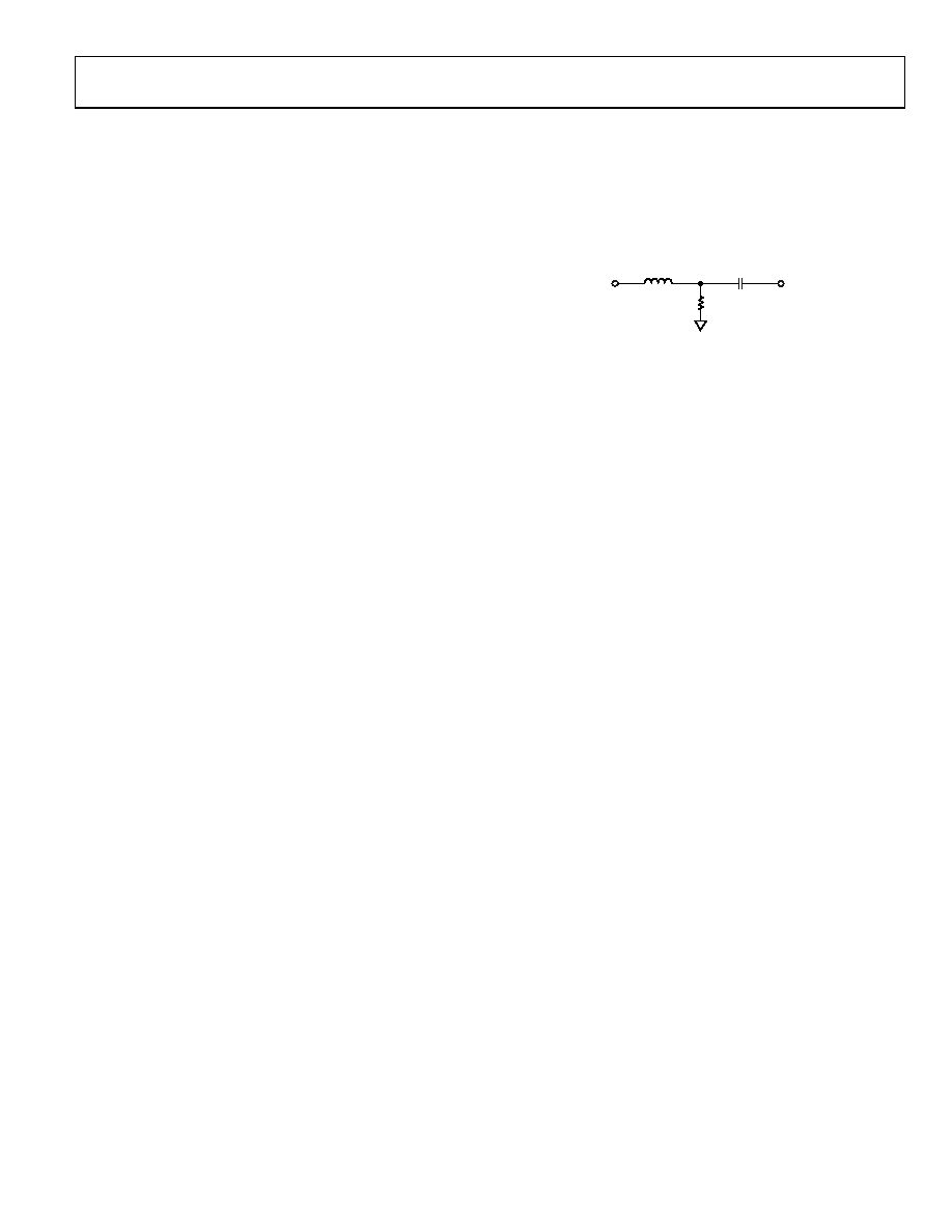
image quality. It has been shown that a small inductor in series
with the input is effective in rolling off the input bandwidth
slightly and providing a high quality signal over a wider range
of conditions. Using a Fair-Rite #2508051217Z0 High Speed
Signal Chip Bead inductor in the circuit of Figure 3 gives good
results in most applications.
RGB
INPUT
RAIN
GAIN
BAIN
47nF
75
04799-0-003
Figure 3. Analog Input Interface Circuit
HSYNC, VSYNC INPUTS
The interface also takes a horizontal sync signal, which is used
to generate the pixel clock and clamp timing. This can be either
a sync signal directly from the graphics source, or a preproc-
essed TTL or CMOS level signal.
The Hsync input includes a Schmitt trigger buffer for immunity
to noise and signals with long rise times. In typical PC-based
graphic systems, the sync signals are simply TTL-level drivers
feeding unshielded wires in the monitor cable. As such, no
termination is required.
SERIAL CONTROL PORT
The serial control port is designed for 3.3 V logic. If there are
5 V drivers on the bus, these pins should be protected with
150 series resistors placed between the pull-up resistors and
the input pins.
OUTPUT SIGNAL HANDLING
The digital outputs are designed and specified to operate from a
3.3 V power supply (VDD). They can also work with a VDD as low
as 2.5 V for compatibility with other 2.5 V logic.
CLAMPING
RGB Clamping
To properly digitize the incoming signal, the dc offset of the
input must be adjusted to fit the range of the on-board A/D
converters.
Most graphics systems produce RGB signals with black at
ground and white at approximately 0.75 V. However, if sync
signals are embedded in the graphics, the sync tip is often at
ground and black is at 300 mV. Then white is at approximately
1.0 V. Some common RGB line amplifier boxes use emitter-
follower buffers to split signals and increase drive capability.
This introduces a 700 mV dc offset to the signal, which must be
removed for proper capture by the AD9985.
The key to clamping is to identify a portion (time) of the signal
when the graphic system is known to be producing black. An
offset is then introduced which results in the A/D converters
producing a black output (code 00h) when the known black
相关PDF资料 |
PDF描述 |
|---|---|
| AD9882AKSTZ-100 | IC INTERFACE/DVI 100MHZ 100LQFP |
| AD9882KSTZ-100 | IC INTERFACE/DVI 100MHZ 100LQFP |
| MS27473E16B55PA | CONN PLUG 55POS STRAIGHT W/PINS |
| LTC4305IGN#TR | IC BUFFER BUS 2WR ADDRESS 16SSOP |
| VI-B43-IW-F2 | CONVERTER MOD DC/DC 24V 100W |
相关代理商/技术参数 |
参数描述 |
|---|---|
| AD9985KST-110 | 制造商:Analog Devices 功能描述:110 MSPS/140 MSPS ANLG INTRFC FOR FLAT PNL DISPLAYS 80LQFP - Bulk |
| AD9985KSTZ-110 | 功能描述:IC INTERFACE 8BIT 110MSPS 80LQFP RoHS:是 类别:集成电路 (IC) >> 接口 - 专用 系列:- 特色产品:NXP - I2C Interface 标准包装:1 系列:- 应用:2 通道 I²C 多路复用器 接口:I²C,SM 总线 电源电压:2.3 V ~ 5.5 V 封装/外壳:16-TSSOP(0.173",4.40mm 宽) 供应商设备封装:16-TSSOP 包装:剪切带 (CT) 安装类型:表面贴装 产品目录页面:825 (CN2011-ZH PDF) 其它名称:568-1854-1 |
| AD9985KSTZ-140 | 功能描述:IC INTERFACE 8BIT 140MSPS 80LQFP RoHS:是 类别:集成电路 (IC) >> 接口 - 专用 系列:- 标准包装:3,000 系列:- 应用:PDA,便携式音频/视频,智能电话 接口:I²C,2 线串口 电源电压:1.65 V ~ 3.6 V 封装/外壳:24-WQFN 裸露焊盘 供应商设备封装:24-QFN 裸露焊盘(4x4) 包装:带卷 (TR) 安装类型:表面贴装 产品目录页面:1015 (CN2011-ZH PDF) 其它名称:296-25223-2 |
| AD9990 | 制造商:AD 制造商全称:Analog Devices 功能描述:Dual Channel, 14-Bit CCD Signal Processor with V-Driver and Precision Timing |
| AD9990BBCZ | 功能描述:IC CCD SGNL PROCESSOR 112CSPBGA RoHS:是 类别:集成电路 (IC) >> 接口 - 传感器和探测器接口 系列:- 其它有关文件:Automotive Product Guide 产品培训模块:Lead (SnPb) Finish for COTS Obsolescence Mitigation Program 标准包装:74 系列:- 类型:触控式传感器 输入类型:数字 输出类型:数字 接口:JTAG,串行 电流 - 电源:100µA 安装类型:表面贴装 封装/外壳:20-TSSOP(0.173",4.40mm 宽) 供应商设备封装:20-TSSOP 包装:管件 |
发布紧急采购,3分钟左右您将得到回复。