- 您现在的位置:买卖IC网 > PDF目录11767 > AD9985BSTZ-110 (Analog Devices Inc)IC INTERFACE 8BIT 110MSPS 80LQFP PDF资料下载
参数资料
| 型号: | AD9985BSTZ-110 |
| 厂商: | Analog Devices Inc |
| 文件页数: | 5/32页 |
| 文件大小: | 0K |
| 描述: | IC INTERFACE 8BIT 110MSPS 80LQFP |
| 标准包装: | 1 |
| 应用: | 视频 |
| 接口: | 串行 |
| 电源电压: | 2.2 V ~ 3.45 V |
| 封装/外壳: | 80-LQFP |
| 供应商设备封装: | 80-LQFP(14x14) |
| 包装: | 管件 |
| 安装类型: | 表面贴装 |
第1页第2页第3页第4页当前第5页第6页第7页第8页第9页第10页第11页第12页第13页第14页第15页第16页第17页第18页第19页第20页第21页第22页第23页第24页第25页第26页第27页第28页第29页第30页第31页第32页
AD9985
Rev. 0 | Page 13 of 32
offset errors in its own ADC channels as well as any offset
errors present on the incoming graphics or video signals.
To activate the auto-offset mode, set Register 1Dh, Bit 7 to 1.
Next, the target code registers (19h through 1Bh) must be
programmed. The values programmed into the target code
registers should be the output code desired from the AD9985
during the back porch reference time. For example, for RGB
signals, all three registers would normally be programmed to
code 1, while for YPbPr signals the green (Y) channel would
normally be programmed to code 1 and the blue and red
channels (Pb and Pr) would normally be set to 128. Any target
code value between 1 and 254 can be set, although the AD9985’s
offset range may not be able to reach every value. Intended
target code values range from (but are not limited to) 1 to 40
when ground clamping and 90 to 170 when midscale clamping.
The ability to program a target code for each channel gives
users a large degree of freedom and flexibility. While in most
cases all channels will be set to either 1 or 128, the flexibility to
select other values allows for the possibility of inserting
intentional skews between channels. It also allows for the ADC
range to be skewed so that voltages outside of the normal range
can be digitized. (For example, setting the target code to 40
would allow the sync tip, which is normally below black level, to
be digitized and evaluated.)
Lastly, when in auto offset mode, the manual offset registers
(0Bh to 0Dh) have new functionality. The values in these
registers are digitally added to the value of the ADC output. The
purpose of doing this is to match a benefit that is present with
manual offset adjustment. Adjusting these registers is an easy
way to make brightness adjustments. Although some signal
range is lost with this method, it has proven to be a very popular
function. In order to be able to increase and decrease brightness,
the values in these registers in this mode are signed twos
complement. The digital adder is used only when in auto offset
mode. Although it cannot be disabled, setting the offset registers
to all 0’s will effectively disable it by always adding 0.
SYNC-ON-GREEN
The Sync-on-Green input operates in two steps. First, it sets a
baseline clamp level off of the incoming video signal with a
negative peak detector. Second, it sets the sync trigger level to a
programmable level (typically 150 mV) above the negative peak.
The Sync-on-Green input must be ac-coupled to the Green
analog input through its own capacitor, as shown in Figure 5.
The value of the capacitor must be 1 nF ±20%. If Sync-on-
Green is not used, this connection is not required. Note that the
Sync-on-Green signal is always negative polarity.
RAIN
BAIN
GAIN
SOG
47nF
1nF
04799-0-005
Figure 5. Typical Clamp Configuration
CLOCK GENERATION
A phase-locked loop (PLL) is employed to generate the pixel
clock. In this PLL, the Hsync input provides a reference
frequency. A voltage controlled oscillator (VCO) generates a
much higher pixel clock frequency. This pixel clock is divided
by the PLL divide value (Registers 01H and 02H) and phase
compared with the Hsync input. Any error is used to shift the
VCO frequency and maintain lock between the two signals.
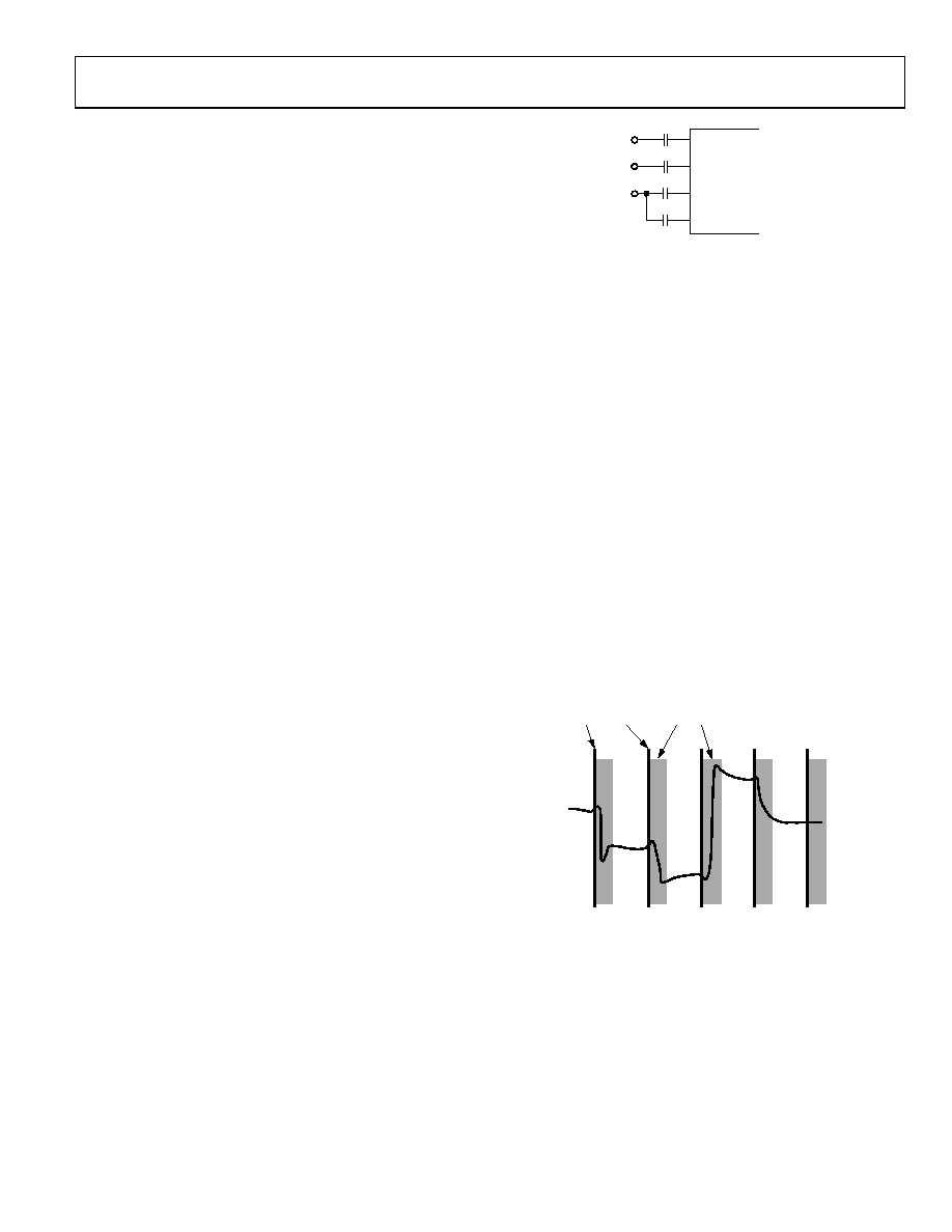
The stability of this clock is a very important element in
providing the clearest and most stable image. During each pixel
time, there is a period during which the signal is slewing from
the old pixel amplitude and settling at its new value. Then there
is a time when the input voltage is stable, before the signal must
slew to a new value (Figure 6). The ratio of the slewing time to
the stable time is a function of the bandwidth of the graphics
DAC and the bandwidth of the transmission system (cable and
termination). It is also a function of the overall pixel rate.
Clearly, if the dynamic characteristics of the system remain
fixed, the slewing and settling time is likewise fixed. This time
must be subtracted from the total pixel period, leaving the stable
period. At higher pixel frequencies, the total cycle time is
shorter, and the stable pixel time becomes shorter as well.
PIXEL CLOCK
INVALID SAMPLE TIMES
04799-0-006
Figure 6. Pixel Sampling Times
Any jitter in the clock reduces the precision with which the
sampling time can be determined, and must also be subtracted
from the stable pixel time.
Considerable care has been taken in the design of the AD9985’s
clock generation circuit to minimize jitter. As indicated in
Figure 7, the clock jitter of the AD9985 is less than 5% of the
total pixel time in all operating modes, making the reduction in
the valid sampling time due to jitter negligible.
相关PDF资料 |
PDF描述 |
|---|---|
| AD9882AKSTZ-100 | IC INTERFACE/DVI 100MHZ 100LQFP |
| AD9882KSTZ-100 | IC INTERFACE/DVI 100MHZ 100LQFP |
| MS27473E16B55PA | CONN PLUG 55POS STRAIGHT W/PINS |
| LTC4305IGN#TR | IC BUFFER BUS 2WR ADDRESS 16SSOP |
| VI-B43-IW-F2 | CONVERTER MOD DC/DC 24V 100W |
相关代理商/技术参数 |
参数描述 |
|---|---|
| AD9985KST-110 | 制造商:Analog Devices 功能描述:110 MSPS/140 MSPS ANLG INTRFC FOR FLAT PNL DISPLAYS 80LQFP - Bulk |
| AD9985KSTZ-110 | 功能描述:IC INTERFACE 8BIT 110MSPS 80LQFP RoHS:是 类别:集成电路 (IC) >> 接口 - 专用 系列:- 特色产品:NXP - I2C Interface 标准包装:1 系列:- 应用:2 通道 I²C 多路复用器 接口:I²C,SM 总线 电源电压:2.3 V ~ 5.5 V 封装/外壳:16-TSSOP(0.173",4.40mm 宽) 供应商设备封装:16-TSSOP 包装:剪切带 (CT) 安装类型:表面贴装 产品目录页面:825 (CN2011-ZH PDF) 其它名称:568-1854-1 |
| AD9985KSTZ-140 | 功能描述:IC INTERFACE 8BIT 140MSPS 80LQFP RoHS:是 类别:集成电路 (IC) >> 接口 - 专用 系列:- 标准包装:3,000 系列:- 应用:PDA,便携式音频/视频,智能电话 接口:I²C,2 线串口 电源电压:1.65 V ~ 3.6 V 封装/外壳:24-WQFN 裸露焊盘 供应商设备封装:24-QFN 裸露焊盘(4x4) 包装:带卷 (TR) 安装类型:表面贴装 产品目录页面:1015 (CN2011-ZH PDF) 其它名称:296-25223-2 |
| AD9990 | 制造商:AD 制造商全称:Analog Devices 功能描述:Dual Channel, 14-Bit CCD Signal Processor with V-Driver and Precision Timing |
| AD9990BBCZ | 功能描述:IC CCD SGNL PROCESSOR 112CSPBGA RoHS:是 类别:集成电路 (IC) >> 接口 - 传感器和探测器接口 系列:- 其它有关文件:Automotive Product Guide 产品培训模块:Lead (SnPb) Finish for COTS Obsolescence Mitigation Program 标准包装:74 系列:- 类型:触控式传感器 输入类型:数字 输出类型:数字 接口:JTAG,串行 电流 - 电源:100µA 安装类型:表面贴装 封装/外壳:20-TSSOP(0.173",4.40mm 宽) 供应商设备封装:20-TSSOP 包装:管件 |
发布紧急采购,3分钟左右您将得到回复。