- 您现在的位置:买卖IC网 > PDF目录378277 > ADC081500 (National Semiconductor Corporation) High Performance, Low Power, 8-Bit, 1.5 GSPS A/D Converter PDF资料下载
参数资料
| 型号: | ADC081500 |
| 厂商: | National Semiconductor Corporation |
| 英文描述: | High Performance, Low Power, 8-Bit, 1.5 GSPS A/D Converter |
| 中文描述: | 高性能,低功耗,8位,1.5 GSPS的A / D转换 |
| 文件页数: | 21/28页 |
| 文件大小: | 830K |
| 代理商: | ADC081500 |
第1页第2页第3页第4页第5页第6页第7页第8页第9页第10页第11页第12页第13页第14页第15页第16页第17页第18页第19页第20页当前第21页第22页第23页第24页第25页第26页第27页第28页
1.0 Functional Description
(Continued)
Input Full-Scale Voltage Adjust
Addr: 3h (0011b)
W only (0x807F)
D15
(MSB)
D14
D13
D12
D11
D10
D9
D8
Adjust Value
D7
D6
1
D5
1
D4
1
D3
1
D2
1
D1
1
D0
1
(LSB)
Bit 15:7
Input Full Scale Voltage Adjust Value. The
input full-scale voltage or gain of the ADC is
adjusted linearly and monotonically with a 9
bit data value. The adjustment range is
±
20% of the nominal 700 mV
P-P
differential
value.
0000 0000 0
560mV
P-P
1000 0000 0
Default Value
1111 1111 1
840mV
P-P
For best performance, it is recommended
that the value in this field be limited to the
range of 0110 0000 0b to 1110 0000 0b. i.e.,
limit the amount of adjustment to
±
15%. The
remaining
±
5% headroom allows for the
ADC’s own full scale variation. A gain
adjustment
does
re-calibration.
POR State: 1000 0000 0b (no adjustment)
Must be set to 1b
700mV
P-P
not
require
ADC
Bits 6:0
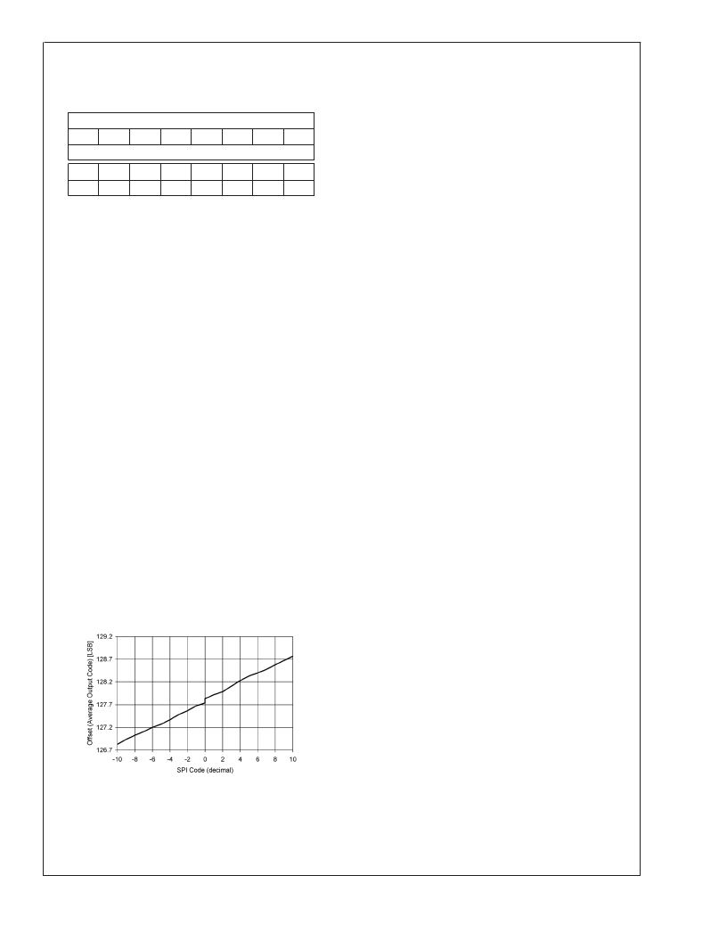
1.4.1 Note Regarding Extended Mode Offset Correction
When using the Input Offset Adjust register, the following
information should be noted.
For offset values of +0000 0000 and -0000 0000, the actual
offset is not the same. By changing only the sign bit in this
case, an offset step in the digital output code of about 1/10th
of an LSB is experienced. This is shown more clearly in the
Figure below.
1.5 MULTIPLE ADC SYNCHRONIZATION
The ADC081500 has the capability to precisely reset its
sampling clock input to DCLK output relationship as deter-
mined by the user-supplied DCLK_RST pulse. This allows
multiple ADCs in a system to have their DCLK (and data)
outputs transition at the same time with respect to the shared
CLK input that they all use for sampling.
The DCLK_RST signal must observe some timing require-
ments that are shown in
Figure 6
,
Figure 7
and
Figure 8
of
the Timing Diagrams. The DCLK_RST pulse must be of a
minimum width and its deassertion edge must observe setup
and hold times with respect to the CLK input rising edge.
These times are specified in the AC Electrical Characteris-
tics Table.
The DCLK_RST signal can be asserted asynchronous to the
input clock. If DCLK_RST is asserted, the DCLK output is
immediately held in a designated state. The state in which
DCLK is held during the reset period is determined by the
mode of operation (SDR/DDR) and the setting of the Output
Edge configuration pin or bit. (Refer to
Figure 6
,
Figure 7
and
Figure 8
for the DCLK reset state conditions). Therefore,
depending upon when the DCLK_RST signal is asserted,
there may be a narrow pulse on the DCLK line during this
reset event. When the DCLK_RST signal is de-asserted in
synchronization with the CLK rising edge, the next CLK
falling edge synchronizes the DCLK output with those of
other ADC081500s in the system. The DCLK output is en-
abled again after a constant delay (relative to the input clock
frequency) which is equal to the CLK input to DCLK output
delay (t
). The device always exhibits this delay character-
istic in normal operation.
The DCLK-RST pin should NOT be brought high while the
calibration process is running (while CalRun is high). Doing
so could cause a digital glitch in the digital circuitry, resulting
in corruption and invalidation of the calibration.
2.0 Applications Information
2.1 THE REFERENCE VOLTAGE
The voltage reference for the ADC081500 is derived from a
1.254V bandgap reference, a buffered version of which is
made available at pin 31, V
BG
for user convenience and has
an output current capability of
±
100 μA. This reference
voltage should be buffered if more current is required.
The internal bandgap-derived reference voltage has a nomi-
nal value of 650 mV or 870 mV, as determined by the FSR
pin and described in Section 1.1.4.
There is no provision for the use of an external reference
voltage, but the full-scale input voltage can be adjusted
through a Configuration Register in the Extended Control
mode, as explained in Section 1.2.
Differential input signals up to the chosen full-scale level will
be digitized to 8 bits. Signal excursions beyond the full-scale
range will be clipped at the output. These large signal excur-
sions will also activate the OR output for the time that the
signal is out of range. See Section 2.2.2.
One extra feature of the V
pin is that it can be used to
raise the common mode voltage level of the LVDS outputs.
The output offset voltage (V
) is typically 800mV when the
V
pin is used as an output or left unconnected. To raise
the LVDS offset voltage to a typical value of 1200mV the V
BG
pin can be connected directly to the supply rails.
2.2 THE ANALOG INPUT
The analog input is a differential one to which the signal
source may be a.c. coupled or d.c. coupled. The full-scale
input range is selected with the FSR pin to be 650 mV
P-P
or
870 mV
P-P
, or can be adjusted to values between 560 mV
P-P
20153130
FIGURE 10. Extended Mode Offset Behaviour
A
www.national.com
21
相关PDF资料 |
PDF描述 |
|---|---|
| ADC081500CIYB | High Performance, Low Power, 8-Bit, 1.5 GSPS A/D Converter |
| ADC081500EVAL | High Performance, Low Power, 8-Bit, 1.5 GSPS A/D Converter |
| ADC08161 | 500 ns A/D Converter with S/H Function and 2.5V Bandgap Reference(500ns带S/H功能和2.5V带隙参考的A/D转换器) |
| ADC08161CIWM | 500 ns A/D Converter with S/H Function and 2.5V Bandgap Reference |
| ADC0816 | 8-BitμP Compatible A/D Converters with 16-Channel Multiplexer(带16通道多路器的8位μP兼容A/D转换器) |
相关代理商/技术参数 |
参数描述 |
|---|---|
| ADC081500_06 | 制造商:NSC 制造商全称:National Semiconductor 功能描述:High Performance, Low Power, 8-Bit, 1.5 GSPS A/D Converter |
| ADC081500_09 | 制造商:NSC 制造商全称:National Semiconductor 功能描述:High Performance, Low Power, 8-Bit, 1.5 GSPS A/D Converter |
| ADC081500CIYB | 功能描述:模数转换器 - ADC RoHS:否 制造商:Texas Instruments 通道数量:2 结构:Sigma-Delta 转换速率:125 SPs to 8 KSPs 分辨率:24 bit 输入类型:Differential 信噪比:107 dB 接口类型:SPI 工作电源电压:1.7 V to 3.6 V, 2.7 V to 5.25 V 最大工作温度:+ 85 C 安装风格:SMD/SMT 封装 / 箱体:VQFN-32 |
| ADC081500CIYB/NOPB | 功能描述:模数转换器 - ADC RoHS:否 制造商:Texas Instruments 通道数量:2 结构:Sigma-Delta 转换速率:125 SPs to 8 KSPs 分辨率:24 bit 输入类型:Differential 信噪比:107 dB 接口类型:SPI 工作电源电压:1.7 V to 3.6 V, 2.7 V to 5.25 V 最大工作温度:+ 85 C 安装风格:SMD/SMT 封装 / 箱体:VQFN-32 |
| ADC081500DEV | 制造商:NSC 制造商全称:National Semiconductor 功能描述:High Performance, Low Power, 8-Bit, 1.5 GSPS A/D Converter |
发布紧急采购,3分钟左右您将得到回复。