- 您现在的位置:买卖IC网 > PDF目录378277 > ADC081500 (National Semiconductor Corporation) High Performance, Low Power, 8-Bit, 1.5 GSPS A/D Converter PDF资料下载
参数资料
| 型号: | ADC081500 |
| 厂商: | National Semiconductor Corporation |
| 英文描述: | High Performance, Low Power, 8-Bit, 1.5 GSPS A/D Converter |
| 中文描述: | 高性能,低功耗,8位,1.5 GSPS的A / D转换 |
| 文件页数: | 23/28页 |
| 文件大小: | 830K |
| 代理商: | ADC081500 |
第1页第2页第3页第4页第5页第6页第7页第8页第9页第10页第11页第12页第13页第14页第15页第16页第17页第18页第19页第20页第21页第22页当前第23页第24页第25页第26页第27页第28页
2.0 Applications Information
(Continued)
The 100 Ohm external resistor placed accross the output
terminals of the balun in parallel with the ADC081500’s
on-chip 100 Ohm resistor makes a 50 Ohms differential
impedance at the balun output. Or, 25 Ohms to virtual
ground at each of the balun output terminals.
Looking into the balun, the source sees the impedance of the
first coil in series with the impedance at the output of that
coil. Since the transformer has a 1:1 turns ratio, the imped-
ance across the first coil is exactly the same as that at the
output of the second coil, namely 25 Ohms to virtual ground.
So, the 25 Ohms across the first coil in series with the 25
Ohms at its output gives 50 Ohms total impedance to match
the source.
2.2.2 Out Of Range (OR) Indication
When the conversion result is clipped the Out of Range
output is activated such that OR+ goes high and OR- goes
low. This output is active as long as accurate data on the
output bus would be outside the range of 00h to FFh.
2.2.3 Full-Scale Input Range
As with all A/D Converters, the input range is determined by
the value of the ADC’s reference voltage. The reference
voltage of the ADC081500 is derived from an internal band-
gap reference. The FSR pin controls the effective reference
voltage of theADC081500 such that the differential full-scale
input range at the analog inputs is 870 mV
P-P
with the FSR
pin high, or is 650 mV
P-P
with FSR pin low. Best SNR is
obtained with FSR high, but better distortion and SFDR are
obtained with the FSR pin low.
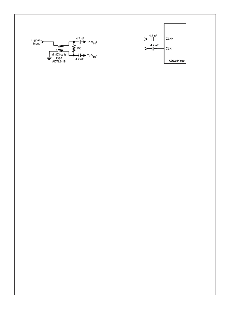
2.3 THE CLOCK INPUTS
The ADC081500 has differential LVDS clock inputs, CLK+
and CLK-, which must be driven with an a.c. coupled, differ-
ential clock signal.Although theADC081500 is tested and its
performance is guaranteed with a differential 1.5 GHz clock,
it typically will function well with input clock frequencies
indicated in the Electrical Characteristics Table. The clock
inputs are internally terminated and biased. The input clock
signal must be capacitively coupled to the clock pins as
indicated in
Figure 14
.
Operation up to the sample rates indicated in the Electrical
Characteristics Table is typically possible if the maximum
ambient temperatures indicated are not exceeded. Operat-
ing at higher sample rates than indicated for the given am-
bient temperature may result in reduced device reliability
and product lifetime. This is because of the higher power
consumption and die temperatures at high sample rates.
Important also for reliability is proper thermal management .
See Section 2.6.2.
The differential input clock line pair should have a character-
istic impedance of 100
and (when using a balun), be
terminated at the clock source in that (100
) characteristic
impedance. The input clock line should be as short and as
direct as possible. The ADC081500 clock input is internally
terminated with an untrimmed 100
resistor.
Insufficient input clock levels will result in poor dynamic
performance. Excessively high input clock levels could
cause a change in the analog input offset voltage. To avoid
these problems, keep the input clock level within the range
specified in the Electrical Characteristics Table.
The low and high times of the input clock signal can affect
the performance of any A/D Converter. The ADC081500
features a duty cycle clock correction circuit which can main-
tain performance over the temperature range of operation.
The ADC will meet its performance specification if the input
clock high and low times are maintained within the range
(20/80% ratio) as specified in the Electrical Characteristics
Table.
High
speed,
high
performance
ADC081500 require a very stable input clock signal with
minimum phase noise or jitter. ADC jitter requirements are
defined by the ADC resolution (number of bits), maximum
ADC input frequency and the input signal amplitude relative
to the ADC input full scale range. The maximum jitter (the
sum of the jitter from all sources) allowed to prevent a
jitter-induced reduction in SNR is found to be
t
J(MAX)
= (V
IN(P-P)
/V
INFSR
) x (1/(2
(N+1)
x
π
x f
IN
))
where t
J(MAX)
is the rms total of all jitter sources in seconds,
V
is the
full-scale range of the ADC, "N" is the ADC resolution in bits
and f
is the maximum input frequency, in Hertz, to the ADC
analog input.
Note that the maximum jitter described above is the arith-
metic sum of the jitter from all sources, including that in the
ADC input clock, that added by the system to the ADC input
clock and input signals and that added by the ADC itself.
Since the effective jitter added by the ADC is beyond user
control, the best the user can do is to keep the sum of the
externally added input clock jitter and the jitter added by the
analog circuitry to the analog signal to a minimum.
Input clock amplitudes above those specified in the Electrical
Characteristics Table may result in increased input offset
voltage. This would cause the converter to produce an out-
put code other than the expected 127/128 when both input
pins are at the same potential.
ADCs
such
as
the
20153143
FIGURE 13. Single-Ended to Differential signal
conversion with a balun-connected transformer
20153147
FIGURE 14. Differential (LVDS) Input Clock Connection
A
www.national.com
23
相关PDF资料 |
PDF描述 |
|---|---|
| ADC081500CIYB | High Performance, Low Power, 8-Bit, 1.5 GSPS A/D Converter |
| ADC081500EVAL | High Performance, Low Power, 8-Bit, 1.5 GSPS A/D Converter |
| ADC08161 | 500 ns A/D Converter with S/H Function and 2.5V Bandgap Reference(500ns带S/H功能和2.5V带隙参考的A/D转换器) |
| ADC08161CIWM | 500 ns A/D Converter with S/H Function and 2.5V Bandgap Reference |
| ADC0816 | 8-BitμP Compatible A/D Converters with 16-Channel Multiplexer(带16通道多路器的8位μP兼容A/D转换器) |
相关代理商/技术参数 |
参数描述 |
|---|---|
| ADC081500_06 | 制造商:NSC 制造商全称:National Semiconductor 功能描述:High Performance, Low Power, 8-Bit, 1.5 GSPS A/D Converter |
| ADC081500_09 | 制造商:NSC 制造商全称:National Semiconductor 功能描述:High Performance, Low Power, 8-Bit, 1.5 GSPS A/D Converter |
| ADC081500CIYB | 功能描述:模数转换器 - ADC RoHS:否 制造商:Texas Instruments 通道数量:2 结构:Sigma-Delta 转换速率:125 SPs to 8 KSPs 分辨率:24 bit 输入类型:Differential 信噪比:107 dB 接口类型:SPI 工作电源电压:1.7 V to 3.6 V, 2.7 V to 5.25 V 最大工作温度:+ 85 C 安装风格:SMD/SMT 封装 / 箱体:VQFN-32 |
| ADC081500CIYB/NOPB | 功能描述:模数转换器 - ADC RoHS:否 制造商:Texas Instruments 通道数量:2 结构:Sigma-Delta 转换速率:125 SPs to 8 KSPs 分辨率:24 bit 输入类型:Differential 信噪比:107 dB 接口类型:SPI 工作电源电压:1.7 V to 3.6 V, 2.7 V to 5.25 V 最大工作温度:+ 85 C 安装风格:SMD/SMT 封装 / 箱体:VQFN-32 |
| ADC081500DEV | 制造商:NSC 制造商全称:National Semiconductor 功能描述:High Performance, Low Power, 8-Bit, 1.5 GSPS A/D Converter |
发布紧急采购,3分钟左右您将得到回复。